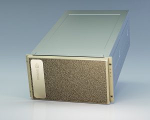
NVIDIA Tesla M40 12GB GPU Accelerator (Maxwell GM200) Up Close

With the release of Tesla M40, NVIDIA continues to diversify its professional compute GPU lineup. Designed specifically for Deep Learning applications, the M40 provides 7 TFLOPS of single-precision floating point performance and 12GB of high-speed GDDR5 memory. It works extremely well with the popular Deep Learning software frameworks and may also find its way into other industries that need single-precision accuracy.

The Tesla M40 is also notable for being the first Tesla GPU to be based upon NVIDIA’s “Maxwell” GPU architecture. “Maxwell” provides excellent performance per watt, as evidenced by the fact that this GPU provides 7 TFLOPS within a 250W power envelope.

Maximum single-GPU performance: Tesla M40 12GB GPU

Available in Microway NumberSmasher GPU Servers and GPU Clusters

Photo of the NVIDIA Tesla M40 12GB GPU Accelerator

Specifications

  • 3072 CUDA GPU cores (GM200)
  • 7.0 TFLOPS single; 0.21 TFLOPS double-precision
  • 12GB GDDR5 memory
  • Memory bandwidth up to 288 GB/s
  • PCI-E x16 Gen3 interface to system
  • Dynamic GPU Boost for optimal clock speeds
  • Passive heatsink design for installation in qualified GPU servers

As with all other modern Tesla GPUs, you should expect it to be able to max out the PCI-E 3.0 bus to achieve ~12GB/sec of data transfers between the system and each GPU:

Continue reading

Deep Learning Frameworks: A Survey of TensorFlow, Torch, Theano, Caffe, Neon, and the IBM Machine Learning Stack

The art and science of training neural networks from large data sets in order to make predictions or classifications has experienced a major transition over the past several years. Through popular and growing interest from scientists and engineers, this field of data analysis has come to be called deep learning. Put succinctly, deep learning is the ability of machine learning algorithms to acquire feature hierarchies from data and then persist those features within multiple non-linear layers which comprise the machine’s learning center, or neural network.

Two years ago, questions were mainly about what deep learning is, and how it might be applied to problems in science, engineering, and finance. Over the past year, however, the climate of interest has changed from a curiosity about what deep learning is, and into a focus on acquiring hardware and software in order to apply deep learning frameworks to specific problems across a wide range of disciplines.

The current major deep learning frameworks will be examined here and compared, across various features, such as native language of framework, multi-GPU support, and aspects of usability.

Continue reading

Keras and Theano Deep Learning Frameworks

Theano_Keras_Blog_masthead_flattened_masthead

Here we will explore how to use the Theano and Keras Python frameworks for designing neural networks in order to accomplish specific classification tasks. In the process, we will see how Keras offers a great amount of leverage and flexibility in designing neural nets. In particular, we will examine two active areas of research: classification of textual and image data.

Continue reading

Caffe Deep Learning Tutorial using NVIDIA DIGITS on Tesla K80 & K40 GPUs

NVIDIA DIGITS Deep Learning Tutorial

In this Caffe deep learning tutorial, we will show how to use DIGITS in order to train a classifier on a small image set.  Along the way, we’ll see how to adjust certain run-time parameters, such as the learning rate, number of training epochs, and others, in order to tweak and optimize the network’s performance.  Other DIGITS features will be introduced, such as starting a training run using the network weights derived from a previous training run, and using a completed classifier from the command line.

Continue reading

DDR4 RDIMM and LRDIMM Performance Comparison

Recently, while carrying out memory testing in our integration lab, Lead Systems Integrator, Rick Warner,  was able to clearly identify when it is appropriate to choose load-reduced DIMMs (LRDIMM) and when it is appropriate to choose registered DIMMs (RDIMM) for servers running large amounts of DDR4 RAM (i.e., 256 Gigabytes and greater). The critical factors to consider are latency, speed, and capacity, along with what your computing objectives are with respect to them.

Misconceptions on Load Reduced DIMM Performance

Load-reduced DIMMs were built so that high-speed memory controllers in CPUs could drive larger quantities of memory. Thus, it’s often assumed that LRDIMMs will offer the best performance for memory-dense servers. This impression is strengthened by the fact that Intel’s guide for DDR4 memory population shows LRDIMMs running at a higher frequency than RDIMMs (e.g., 2133MHz vs 1866MHz). However, as we’ll show below, there are greater factors at play.

Continue reading

Intel Xeon E5-4600v3 “Haswell” 4-socket CPU Review

Intel has launched new 4-socket Xeon E5-4600v3 CPUs. They are the perfect choice for “just beyond dual socket” system scaling. Leverage them for larger memory capacity, faster memory bandwidth, and higher core-count when you aren’t ready for a multi-system purchase.

Here are a few of the main technical improvements:

  • DDR4-2133 memory support, for increased memory bandwidth
  • Up to 18 cores per socket, faster QPI links up to 9.6GT/sec between sockets
  • Up to 48 DIMMs per server, for a maximum of 3TB memory
  • Haswell core microarchitecture with new instructions

Why pick a 4-socket Xeon E5-4600v3 CPU over a 2 socket solution?

Continue reading

Common PCI-Express Myths for GPU Computing Users

At Microway we design a lot of GPU computing systems. One of the strengths of GPU-compute is the flexibility PCI-Express bus. Assuming the server has appropriate power and thermals, it enables us to attach GPUs with no special interface modifications. We can even swap to new GPUs under many circumstances. However, we encounter a lot of misinformation about PCI-Express and GPUs. Here are a number of myths about PCI-E:

1. PCI-Express is controlled through the chipset

No longer in modern Intel CPU-based platforms. Beginning with the Sandy Bridge CPU architecture in 2012 (Xeon E5 series CPUs, Xeon E3 series CPUs, Core i7-2xxx and newer) Intel integrated the PCI-Express controller into the the CPU die itself. Bringing PCI-Express onto the CPU die came with a substantial latency benefit. This was a major change in platform design, and Intel coupled it with the addition of PCI-Express Gen3 support.

Continue reading

Introduction to RAID for HPC Customers

There is a lot of material available on RAID, describing the technologies, the options, and the pitfalls.  However, there isn’t a great deal on RAID from an HPC perspective.  We’d like to provide an introduction to RAID, clear up a few misconceptions, share with you some best practices, and explain what sort of configurations we recommend for different use cases.

What is RAID?

Originally known as Redundant Array of Inexpensive Disks, the acronym is now more commonly considered to stand for Redundant Array of Independent Disks.  The main benefits to RAID are improved disk read/write performance, increased redundancy, and the ability to increase logical volume sizes.

RAID is able to perform these functions primarily through striping, mirroring, and parity.  Striping is when files are broken down into segments, which are then placed on different drives.  Because the files are spread across multiple drives that are running in parallel, performance is improved.  Mirroring is when data is duplicated on the fly across drives.  Parity within the context of RAID refers to when data redundancy is distributed across all drives so that when one or more (depending on the RAID level) drives fail, the data can be reconstructed from the remaining drives. Continue reading

Introducing the NVIDIA Tesla K80 GPU Accelerator (Kepler GK210)

NVIDIA has once again raised the bar on GPU computing with the release of the new Tesla K80 GPU accelerator.  With up to 8.74 TFLOPS of single-precision performance with GPU Boost, the Tesla K80 has massive capability and leading density.

NVIDIA Tesla K80

Here are the important performance specifications:

  • Two GK210 chips on a single PCB
  • 4992 total SMX CUDA cores: 2496 on each chip!
  • Total of 24GB GDDR5 memory; aggregate memory bandwidth of 480GB/sec
  • 5.6 TFLOPS single precision, 1.87 TFLOPS double precision
  • 8.74 TFLOPS single precision, 2.91 TFLOPS double precision with GPU Boost
  • 300W TDP

To achieve this performance, Tesla K80 is really two GPUs in one. This Tesla K80 block diagram illustrates how each GK210 GPU has its own dedicated memory and how they communicate at x16 speeds with the PCIe bus using a PCIe switch:

Tesla K80 block diagram

Continue reading

How to Benchmark GROMACS GPU Acceleration on HPC Clusters

Cropped shot of a GROMACS adh simulation (visualized with VMD)

We know that many of our readers are interested in seeing how molecular dynamics applications perform with GPUs, so we are continuing to highlight various packages. This time we will be looking at GROMACS, a well-established and free-to-use (under GNU GPL) application.  GROMACS is a popular choice for scientists interested in simulating molecular interaction. With NVIDIA Tesla K40 GPUs, it’s common to see 2X and 3X speedups compared to the latest multi-core CPUs.

Continue reading