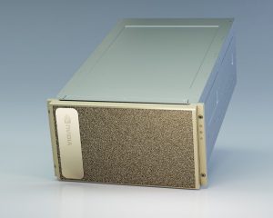
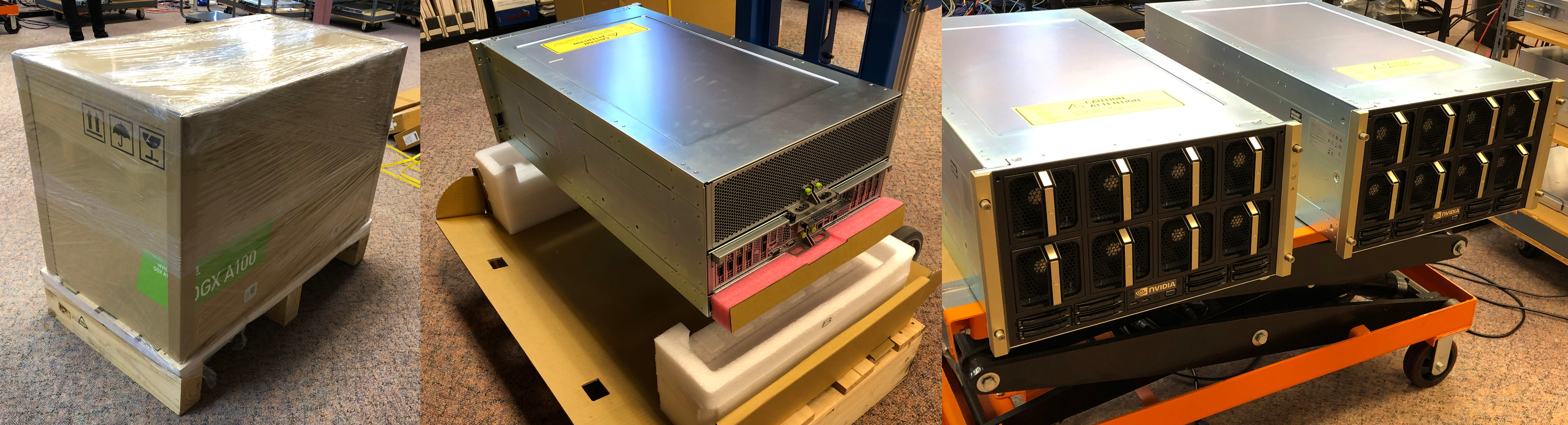
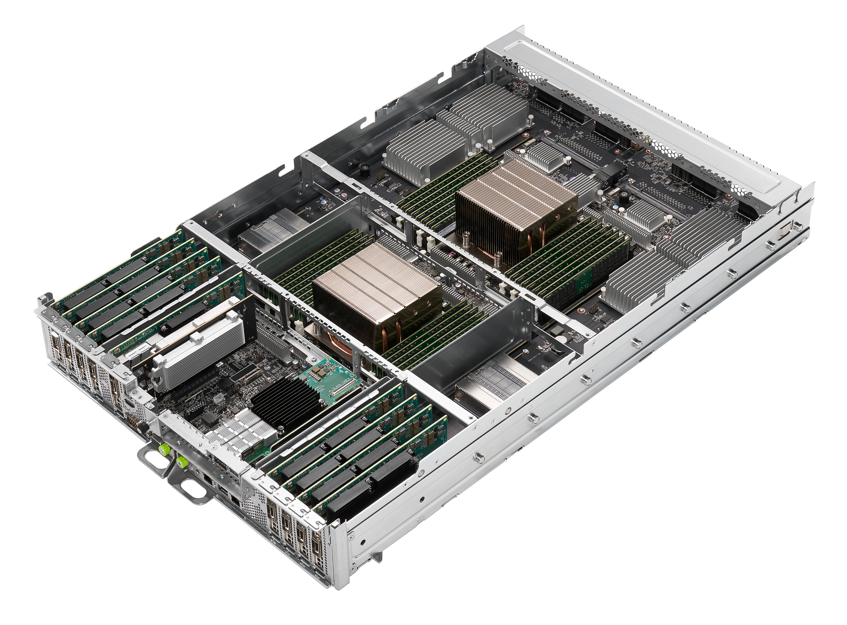
When NVIDIA launched the Ampere GPU architecture, they also launched their new flagship system for HPC and deep learning – the DGX 100. This system offers exceptional performance, but also new capabilities. We’ve seen immediate interest and have already shipped to some of the first adopters. Given our early access, we wanted to share a deeper dive into this impressive new system.
The focus of this NVIDIA DGX™ A100 review is on the hardware inside the system – the server features a number of features & improvements not available in any other type of server at the moment. DGX will be the “go-to” server for 2020. But hardware only tells part of the story, particularly for NVIDIA’s DGX products. NVIDIA employs more software engineers than hardware engineers, so be certain that application and GPU library performance will continue to improve through updates to the DGX Operating System and to the whole catalog of software containers provided through the NGC hub. Expect more details as the year continues.
Overall DGX A100 System Architecture
This new DGX system offers top-bin parts across-the-board. Here’s the high-level overview:
- Dual 64-core AMD EPYC 7742 CPUs
- 1TB DDR4 system memory (upgradeable to 2TB)
- Eight NVIDIA A100 SXM4 GPUs with NVLink
- NVIDIA NVSwitch connectivity between all GPUs
- 15TB high-speed NVMe SSD Scratch Space (upgradeable to 30TB)
- Eight Mellanox 200Gbps HDR InfiniBand/Ethernet Single-Port Adapters
- One or Two Mellanox 200Gbps Ethernet Dual-Port Adapter(s)
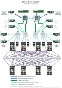
As you’ll see from the block diagram, there is a lot to break down within such a complex system. Though it’s a very busy diagram, it becomes apparent that the design is balanced and well laid out. Breaking down the connectivity within DGX A100 we see:
- The eight NVIDIA A100 GPUs are depicted at the bottom of the diagram, with each GPU fully linked to all other GPUs via six NVSwitches
- Above the GPUs are four PCI-Express switches which act as nexuses between the GPUs and the rest of the system devices
- Linking into the PCI-E switch nexuses, there are eight 200Gbps network adapters and eight high-speed SSD devices – one for each GPU
- The devices are broken into pairs, with 2 GPUs, 2 network adapters, and 2 SSDs per PCI-E nexus
- Each of the AMD EPYC CPUs connects to two of the PCI-E switch nexuses
- At the top of the diagram, each EPYC CPU is shown with a link to system memory and a link to a 200Gbps network adapter
We’ll dig into each aspect of the system in turn, starting with the CPUs and making our way down to the new NVIDIA A100 GPUs. Readers should note that throughput and performance numbers are only useful when put into context. You are encouraged to run the same tests on your existing systems/servers to better understand how the performance of DGX A100 will compare to your existing resources. And as always, reach out to Microway’s DGX experts for additional discussion, review, and design of a holistic solution.
Index of our DGX A100 review:
- AMD EPYC CPUs and System Memory
- High-speed NVMe Storage
- High-Throughput / Low-Latency Communications
- GPU-to-GPU Transfers
- Host-to-Device Transfers
- NVIDIA A100 SXM4 GPUs
- Multi-Instance GPU (MIG)
- DGX A100 Review Summary
AMD EPYC CPUs and System Memory
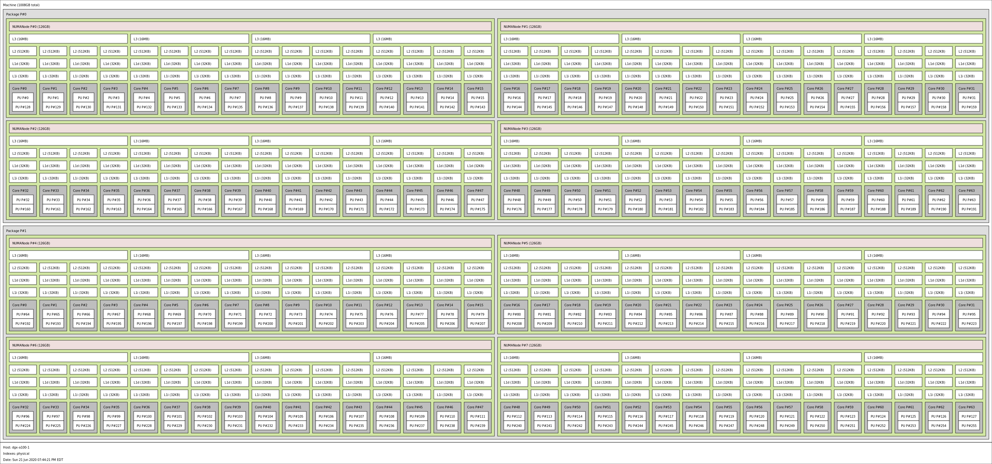
With two 64-core EPYC CPUs and 1TB or 2TB of system memory, the DGX A100 boasts respectable performance even before the GPUs are considered. The architecture of the AMD EPYC “Rome” CPUs is outside the scope of this article, but offers an elegant design of its own. Each CPU provides 64 processor cores (supporting up to 128 threads), 256MB L3 cache, and eight channels of DDR4-3200 memory (which provides the highest memory throughput of any mainstream x86 CPU).
Most users need not dive further, but experts will note that each EPYC 7742 CPU has four NUMA nodes (for a total of eight nodes). This allows best performance for parallelized applications and can also reduce the impact of noisy neighbors. Pairs of GPUs are connected to NUMA nodes 1, 3, 5, and 7. Here’s a snapshot of CPU capabilities from the lscpu utility:
Architecture:        x86_64
CPU(s):              256
Thread(s) per core:  2
Core(s) per socket:  64
Socket(s):           2
CPU MHz:             3332.691
CPU max MHz:         2250.0000
CPU min MHz:         1500.0000
NUMA node0 CPU(s):   0-15,128-143
NUMA node1 CPU(s):   16-31,144-159
NUMA node2 CPU(s):   32-47,160-175
NUMA node3 CPU(s):   48-63,176-191
NUMA node4 CPU(s):   64-79,192-207
NUMA node5 CPU(s):   80-95,208-223
NUMA node6 CPU(s):   96-111,224-239
NUMA node7 CPU(s):   112-127,240-255
High-speed NVMe Storage
Although DGX A100 is designed to support extremely high-speed connectivity to network/cluster storage, it also provides internal flash storage drives. Redundant 2TB NVMe SSDs are provided to host the Operating System. Four non-redundant striped NVMe SSDs provide a 14TB space for scratch storage (which is most frequently used to cache data coming from a centralized storage system).
Here’s how the filesystems look on a fresh DGX A100:
Filesystem      Size  Used Avail Use%    Mounted on
/dev/md0        1.8T   14G  1.7T   1%    /
/dev/md1         14T   25M   14T   1%    /raid
The industry is trending towards Linux software RAID rather than hardware controllers for NVMe SSDs (as such controllers present too many performance bottlenecks). Here’s what the above md0 and md1 arrays look like when healthy:
md0 : active raid1 nvme1n1p2[0] nvme2n1p2[1]
      1874716672 blocks super 1.2 [2/2] [UU]
      bitmap: 1/14 pages [4KB], 65536KB chunk

md1 : active raid0 nvme5n1[2] nvme3n1[1] nvme4n1[3] nvme0n1[0]
      15002423296 blocks super 1.2 512k chunks
It’s worth noting that although all the internal storage devices are high-performance, the scratch drives making up the /raid filesystem support the newer PCI-E generation 4.0 bus which doubles I/O throughput. NVIDIA leads the pack here, as they’re the first we’ve seen to be shipping these new super-fast SSDs.
High-Throughput and Low-Latency Communications with Mellanox 200Gbps
Depending upon the deployment, nine or ten Mellanox 200Gbps adapters are present in each DGX A100. These adapters support Mellanox VPI, which enables each port to be configured for 200G Ethernet or HDR InfiniBand. Though Ethernet is particularly prevalent in particular sectors (healthcare and other industry verticals), InfiniBand tends to be the mode of choice when highest performance is required.
In practice, a common configuration is for the GPU-adjacent adapters be connected to an InfiniBand fabric (which allows for high-performance RDMA GPU-Direct and Magnum IO communications). The adapter(s) attached to the CPUs are then used for Ethernet connectivity (often meeting the speed of the existing facility Ethernet, which might be any one of 10GbE, 25GbE, 40GbE, 50GbE, 100GbE, or 200GbE).
Leveraging the fast PCI-E 4.0 bus available in DGX A100, each 200Gbps port is able to push up to 24.6GB/s of throughput (with latencies typically ranging from 1.09 to 202 microseconds as measured by OSU’s osu_bw and osu_latency benchmarks). Thus, a properly tuned application running across a cluster of DGX systems could push upwards of 200 gigabytes per second to the fabric!
GPU-to-GPU Transfers with NVSwitch and NVLink
NVIDIA built a new generation of NVIDIA NVLink into the NVIDIA A100 GPUs, which provides double the throughput of NVLink in the previous “Volta” generation. Each NVIDIA A100 GPU supports up to 300GB/s throughput (600GB/s bidirectional). Combined with NVSwitch, which connects each GPU to all other GPUs, the DGX A100 provides full connectivity between all eight GPUs.
Running NVIDIA’s p2pBandwidthLatencyTest utility, we can examine the transfer speeds between each set of GPUs:
Unidirectional P2P=Enabled Bandwidth (P2P Writes) Matrix (GB/s)
   D\D     0      1      2      3      4      5      6      7
     0 1180.14 254.47 258.80 254.13 257.67 247.62 257.21 251.53
     1 255.35 1173.05 261.04 243.97 257.09 247.20 258.64 257.51
     2 253.79 260.46 1155.70 241.66 260.23 245.54 259.49 255.91
     3 256.19 261.29 253.87 1142.18 257.59 248.81 250.10 259.44
     4 252.35 260.44 256.82 249.11 1169.54 252.46 257.75 255.62
     5 256.82 257.64 256.37 249.76 255.33 1142.18 259.72 259.95
     6 261.78 260.25 261.81 249.77 258.47 248.63 1173.05 255.47
     7 259.47 261.96 253.61 251.00 259.67 252.21 254.58 1169.54
The above values show GPU-to-GPU transfer throughput ranging from 247GB/s to 262GB/s. Running the same test in bidirectional mode shows results between 473GB/s and 508GB/s. Execution within the same GPU (running down the diagonal) shows data rates around 1,150GB/s.
Turning to latencies, we see fairly uniform communication times between GPUs at ~3 microseconds:
P2P=Enabled Latency (P2P Writes) Matrix (us)
   GPU     0      1      2      3      4      5      6      7
     0   2.63   2.98   2.99   2.96   3.01   2.96   2.96   3.00
     1   3.02   2.59   2.96   3.00   3.03   2.96   2.96   3.03
     2   3.02   2.95   2.51   2.97   3.03   3.04   3.02   2.96
     3   3.05   3.01   2.99   2.49   2.99   2.98   3.06   2.97
     4   2.88   2.88   2.95   2.87   2.39   2.87   2.90   2.88
     5   2.87   2.95   2.89   2.87   2.94   2.49   2.87   2.87
     6   2.89   2.86   2.86   2.88   2.93   2.93   2.53   2.88
     7   2.90   2.90   2.94   2.89   2.87   2.87   2.87   2.54

   CPU     0      1      2      3      4      5      6      7
     0   4.54   3.86   3.94   4.10   3.92   3.93   4.07   3.92
     1   3.99   4.52   4.00   3.96   3.98   4.05   3.92   3.93
     2   4.09   3.99   4.65   4.01   4.00   4.01   4.00   3.97
     3   4.10   4.01   4.03   4.59   4.02   4.03   4.04   3.95
     4   3.89   3.91   3.83   3.88   4.29   3.77   3.76   3.77
     5   4.20   3.87   3.83   3.83   3.89   4.31   3.89   3.84
     6   3.76   3.72   3.77   3.71   3.78   3.77   4.19   3.77
     7   3.86   3.79   3.78   3.78   3.79   3.83   3.81   4.27
As with the bandwidths, the values down the diagonal show execution within that particular GPU. Latencies are lower when executing within a single GPU as there’s no need to hop across the bus to NVSwitch or another GPU. These values show that the same-device latencies are 0.3~0.5 microseconds faster than when communicating with a different GPU via NVSwitch.
Finally, we want to share the full DGX A100 topology as reported by the nvidia-smi topo --matrix utility. While a lot to digest, the main takeaways from this connectivity matrix are the following:
- all GPUs have full NVLink connectivity (12 links each)
- each pair of GPUs is connected to a pair of Mellanox adapters via a
PXBPCI-E switch - each pair of GPUs is closest to a particular set of CPU cores (CPU and NUMA affinity)
	GPU0	GPU1	GPU2	GPU3	GPU4	GPU5	GPU6	GPU7	mlx5_0	mlx5_1	mlx5_2	mlx5_3	mlx5_4	mlx5_5	mlx5_6	mlx5_7	mlx5_8	mlx5_9	CPU Affinity	NUMA Affinity
GPU0	 X 	NV12	NV12	NV12	NV12	NV12	NV12	NV12	PXB	PXB	SYS	SYS	SYS	SYS	SYS	SYS	SYS	SYS	48-63,176-191	3
GPU1	NV12	 X 	NV12	NV12	NV12	NV12	NV12	NV12	PXB	PXB	SYS	SYS	SYS	SYS	SYS	SYS	SYS	SYS	48-63,176-191	3
GPU2	NV12	NV12	 X 	NV12	NV12	NV12	NV12	NV12	SYS	SYS	PXB	PXB	SYS	SYS	SYS	SYS	SYS	SYS	16-31,144-159	1
GPU3	NV12	NV12	NV12	 X 	NV12	NV12	NV12	NV12	SYS	SYS	PXB	PXB	SYS	SYS	SYS	SYS	SYS	SYS	16-31,144-159	1
GPU4	NV12	NV12	NV12	NV12	 X 	NV12	NV12	NV12	SYS	SYS	SYS	SYS	PXB	PXB	SYS	SYS	SYS	SYS	112-127,240-255	7
GPU5	NV12	NV12	NV12	NV12	NV12	 X 	NV12	NV12	SYS	SYS	SYS	SYS	PXB	PXB	SYS	SYS	SYS	SYS	112-127,240-255	7
GPU6	NV12	NV12	NV12	NV12	NV12	NV12	 X 	NV12	SYS	SYS	SYS	SYS	SYS	SYS	PXB	PXB	SYS	SYS	80-95,208-223	5
GPU7	NV12	NV12	NV12	NV12	NV12	NV12	NV12	 X 	SYS	SYS	SYS	SYS	SYS	SYS	PXB	PXB	SYS	SYS	80-95,208-223	5

Legend:
  X    = Self
  SYS  = Connection traversing PCIe as well as the SMP interconnect between NUMA nodes (e.g., QPI/UPI)
  NODE = Connection traversing PCIe as well as the interconnect between PCIe Host Bridges within a NUMA node
  PXB  = Connection traversing multiple PCIe bridges (without traversing the PCIe Host Bridge)
  PIX  = Connection traversing at most a single PCIe bridge
  NV#  = Connection traversing a bonded set of # NVLinks
Host-to-Device Transfer Speeds with PCI-Express generation 4.0
Just as it’s important for the GPUs to be able to communicate with each other, the CPUs must be able to communicate with the GPUs. A100 is the first NVIDIA GPU to support the new PCI-E gen4 bus speed, which doubles the transfer speeds of generation 3. True to expectations, NVIDIA bandwidthTest demonstrates 2X speedups on transfer speeds from the system to each GPU and from each GPU to the system:
 Host to Device Bandwidth, 1 Device(s)
 PINNED Memory Transfers
   Transfer Size (Bytes)	Bandwidth(GB/s)
   32000000			24.7

 Device to Host Bandwidth, 1 Device(s)
 PINNED Memory Transfers
   Transfer Size (Bytes)	Bandwidth(GB/s)
   32000000			26.1
As you might notice, these performance values are right in line with the throughput of each Mellanox 200Gbps adapter. Having eight network adapters with the exact same bandwidth as each of the eight GPUs allows for perfect balance. Data can stream into each GPU from the fabric at line rate (and vice versa).
Diving into the NVIDIA A100 SXM4 GPUs
The DGX A100 is unique in leveraging NVSwitch to provide the full 300GB/s NVLink bandwidth (600GB/s bidirectional) between all GPUs in the system. Although it’s possible to examine a single GPU within this platform, it’s important to keep in mind the context that the GPUs are tightly connected to each other (as well as their linkage to the EPYC CPUs and the Mellanox adapters). The single-GPU information we share below will likely match that shown for A100 SXM4 GPUs in other non-DGX systems. However, their overall performance will depend on the complete system architecture.
To start, here is the ‘brief’ dump of GPU information as provided by nvidia-smi on DGX A100:
+-----------------------------------------------------------------------------+
| NVIDIA-SMI 450.36.06    Driver Version: 450.36.06    CUDA Version: 11.0     |
|-------------------------------+----------------------+----------------------+
| GPU  Name        Persistence-M| Bus-Id        Disp.A | Volatile Uncorr. ECC |
| Fan  Temp  Perf  Pwr:Usage/Cap|         Memory-Usage | GPU-Util  Compute M. |
|                               |                      |               MIG M. |
|===============================+======================+======================|
|   0  A100-SXM4-40GB      On   | 00000000:07:00.0 Off |                    0 |
| N/A   31C    P0    60W / 400W |      0MiB / 40537MiB |      7%      Default |
|                               |                      |             Disabled |
+-------------------------------+----------------------+----------------------+
|   1  A100-SXM4-40GB      On   | 00000000:0F:00.0 Off |                    0 |
| N/A   30C    P0    63W / 400W |      0MiB / 40537MiB |     14%      Default |
|                               |                      |             Disabled |
+-------------------------------+----------------------+----------------------+
|   2  A100-SXM4-40GB      On   | 00000000:47:00.0 Off |                    0 |
| N/A   30C    P0    62W / 400W |      0MiB / 40537MiB |     24%      Default |
|                               |                      |             Disabled |
+-------------------------------+----------------------+----------------------+
|   3  A100-SXM4-40GB      On   | 00000000:4E:00.0 Off |                    0 |
| N/A   29C    P0    58W / 400W |      0MiB / 40537MiB |     23%      Default |
|                               |                      |             Disabled |
+-------------------------------+----------------------+----------------------+
|   4  A100-SXM4-40GB      On   | 00000000:87:00.0 Off |                    0 |
| N/A   34C    P0    62W / 400W |      0MiB / 40537MiB |     23%      Default |
|                               |                      |             Disabled |
+-------------------------------+----------------------+----------------------+
|   5  A100-SXM4-40GB      On   | 00000000:90:00.0 Off |                    0 |
| N/A   33C    P0    60W / 400W |      0MiB / 40537MiB |     23%      Default |
|                               |                      |             Disabled |
+-------------------------------+----------------------+----------------------+
|   6  A100-SXM4-40GB      On   | 00000000:B7:00.0 Off |                    0 |
| N/A   34C    P0    65W / 400W |      0MiB / 40537MiB |     22%      Default |
|                               |                      |             Disabled |
+-------------------------------+----------------------+----------------------+
|   7  A100-SXM4-40GB      On   | 00000000:BD:00.0 Off |                    0 |
| N/A   33C    P0    63W / 400W |      0MiB / 40537MiB |     21%      Default |
|                               |                      |             Disabled |
+-------------------------------+----------------------+----------------------+
The clock speed and power consumption of each GPU will vary depending upon the workload (running low when idle to conserve energy and running as high as possible when executing applications). The idle, default, and max boost speeds are shown below. You will note that memory speeds are fixed at 1215 MHz.
    Clocks
        Graphics                          : 420 MHz (GPU is idle)
        Memory                            : 1215 MHz
    Default Applications Clocks
        Graphics                          : 1095 MHz
        Memory                            : 1215 MHz
    Max Clocks
        Graphics                          : 1410 MHz
        Memory                            : 1215 MHz
Those who have particularly stringent efficiency or power requirements will note that the NVIDIA A100 SXM4 GPU supports 81 different clock speeds between 210 MHz and 1410MHz. Power caps can be set to keep each GPU within preset limits between 100 Watts and 400 Watts. Microway’s post on nvidia-smi for GPU control offers more details for those who need such capabilities.
Each new generation of NVIDIA GPUs introduces new architecture capabilities and adjustments to existing features (such as resizing cache). Some details can be found through the deviceQuery utility, reports the CUDA capabilities of each NVIDIA A100 GPU device:
  CUDA Driver Version / Runtime Version          11.0 / 11.0
  CUDA Capability Major/Minor version number:    8.0
  Total amount of global memory:                 40537 MBytes (42506321920 bytes)
  (108) Multiprocessors, ( 64) CUDA Cores/MP:     6912 CUDA Cores
  GPU Max Clock rate:                            1410 MHz (1.41 GHz)
  Memory Clock rate:                             1215 Mhz
  Memory Bus Width:                              5120-bit
  L2 Cache Size:                                 41943040 bytes
  Maximum Texture Dimension Size (x,y,z)         1D=(131072), 2D=(131072, 65536), 3D=(16384, 16384, 16384)
  Maximum Layered 1D Texture Size, (num) layers  1D=(32768), 2048 layers
  Maximum Layered 2D Texture Size, (num) layers  2D=(32768, 32768), 2048 layers
  Total amount of constant memory:               65536 bytes
  Total amount of shared memory per block:       49152 bytes
  Total shared memory per multiprocessor:        167936 bytes
  Total number of registers available per block: 65536
  Warp size:                                     32
  Maximum number of threads per multiprocessor:  2048
  Maximum number of threads per block:           1024
  Max dimension size of a thread block (x,y,z): (1024, 1024, 64)
  Max dimension size of a grid size    (x,y,z): (2147483647, 65535, 65535)
  Maximum memory pitch:                          2147483647 bytes
  Texture alignment:                             512 bytes
  Concurrent copy and kernel execution:          Yes with 2 copy engine(s)
  Run time limit on kernels:                     No
  Integrated GPU sharing Host Memory:            No
  Support host page-locked memory mapping:       Yes
  Alignment requirement for Surfaces:            Yes
  Device has ECC support:                        Enabled
  Device supports Unified Addressing (UVA):      Yes
  Device supports Managed Memory:                Yes
  Device supports Compute Preemption:            Yes
  Supports Cooperative Kernel Launch:            Yes
  Supports MultiDevice Co-op Kernel Launch:      Yes
In the NVIDIA A100 GPU, NVIDIA increased cache & global memory size, introduced new instruction types, enabled new asynchronous data copy capabilities, and more. More complete information is available in our Knowledge Center article which summarizes the features of the Ampere GPU architecture. However, it could be argued that the biggest architecture change is the introduction of MIG.
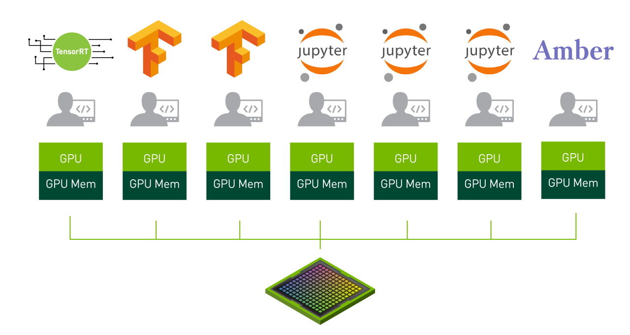
Multi-Instance GPU (MIG)
For years, virtualization has allowed CPUs to be virtually broken into chunks and shared between a wide group of users and/or applications. One physical CPU device might be simultaneously running jobs for a dozen different users. The flexibility and security offered by virtualization has spawned billion dollar businesses and whole new industries.
NVIDIA GPUs have supported multiple users and virtualization for a couple of generations, but NVIDIA A100 GPUs with MIG are the first to support physical separation of those tasks. In essence, one GPU can now be sliced into up to seven distinct hardware instances. Each instance then runs its own completely independent applications with no interruption or “noise” from other applications running on the GPU:
The MIG capabilities are significant enough that we won’t attempt to address them all here. Instead, we’ll highlight the most important aspects of MIG. Readers needing complete implementation details are encouraged to reference NVIDIA’s MIG documentation.
Each GPU can have MIG enabled or disabled (which means a DGX A100 system might have some shared GPUs and some dedicated GPUs). Enabling MIG on a GPU has the following effects:
- One NVIDIA A100 GPU may be split into anywhere between 2 and 7 GPU Instances
- Each of the GPU Instances receives a dedicated set of hardware units: GPU compute resources (including streaming multiprocessors/SMs, and GPU engines such as copy engines or NVDEC video decoders), and isolated paths through the entire memory system (L2 cache, memory controllers, and DRAM address busses, etc)
- Each of the GPU Instances can be further divided into Compute Instances, if desired. Each Compute Instance is provided a set of dedicated compute resources (SMs), but all the Compute Instances within the GPU Instance share the memory and GPU engines (such as the video decoders)
- A unique
CUDA_VISIBLE_DEVICESidentifier will be created for each Compute Instance and the corresponding parent GPU Instance. The identifier follows this convention:MIG-<GPU-UUID>/<GPU instance ID>/<compute instance ID> - Graphics API support (e.g. OpenGL etc.) is disabled
- GPU to GPU P2P (either PCI-Express or NVLink) is disabled
- CUDA IPC across GPU instances is not supported (though IPC across the Compute Instances within one GPU Instance is supported)
Though the above caveats are important to note, they are not expected to be significant pain points in practice. Applications which require NVLink will be workloads that require significant performance and should not be run on a shared GPU. Applications which need to virtualize GPUs for graphical applications are likely to use a different type of NVIDIA GPU.
Also note that the caveats don’t extend all the way through the CUDA capabilities and software stack. The following features are supported when MIG is enabled:
- MIG is transparent to CUDA and existing CUDA programs can run under MIG unchanged
- CUDA MPS is supported on top of MIG
- GPUDirect RDMA is supported when used from GPU Instances
- CUDA debugging (e.g. using cuda-gdb) and memory/race checking (e.g. using cuda-memcheck or compute-sanitizer) is supported
When MIG is fully-enabled on the DGX A100 system, up to 56 separate GPU Instances can be executed simultaneously. That could be 56 unique workloads, 56 separate users each running a Jupyter notebook, or some other combination of users and applications. And if some of the users/workloads have more demanding needs than others, MIG can be reconfigured to issue larger slices of the GPU to those particular applications.
DGX A100 Review Summary
As mentioned at the top, this new hardware is quite impressive, but is only one part of the DGX story. NVIDIA has multiple software stacks to suit the broad range of possible uses for this system. If you’re just getting started, there’s a lot left to learn. Depending upon what you need next, I’d suggest a few different directions:
- If you’re considering a hardware deployment (on-prem or via colo facility), please do contact us and we’ll loop in the appropriate “DGXperts” at NVIDIA to assemble a holistic deployment plan and ensure your project is a success.
- If you’d like to learn more about the NVIDIA “Ampere” architecture consider the following resources:
- If you’d like to learn more about the latest NVIDIA libraries and software tools, look to these resources: