This article provides in-depth discussion and analysis of the 14nm Intel Xeon Processor Scalable Family (formerly codenamed “Skylake-SP” or “Skylake Scalable Processor”). “Skylake-SP” processors replace the previous 14nm “Broadwell” microarchitecture (both the E5 and E7 Xeon families) and are available for sale as of July 11, 2017. Note: these have since been superseded by the “Cascade Lake SP” Intel Xeon Processor Scalable Family CPUs.
Important changes available in Xeon Scalable Processor Family “Skylake-SP” CPUs include:
- Up to 28 processor cores per socket (with options for 4-, 6-, 8-, 10-, 12-, 14-, 16-, 18-, 20-, 24-, and 26-cores)
- Floating Point and Integer Instruction performance improvements:
- New AVX-512 instructions double performance
(up to 16 double-precision FLOPS per cycle per AVX-512 FMA unit) - Up to two AVX-512 FMA units per CPU core (depends upon CPU SKU)
- New AVX-512 instructions double performance
- Memory capacity & performance improvements:
- Six-channel memory controller on each CPU (up from four-channel on previous platforms)
- Support for DDR4 memory speeds up to 2666MHz
- Optional 1.5TB-per-socket system memory support (only available on certain SKUs)
- Faster links between CPU sockets with up to three 10.4GT/s UPI links (replacing the older QPI interconnect)
- More I/O connectivity with 48 lanes of generation 3.0 PCI-Express per CPU (up from 40 lanes)
- Optional 100Gbps Omni-Path fabric integrated into the processor (only available on certain SKUs)
- CPU cores are arranged in an “Uncore” mesh interconnect (replacing the older dual-ring mesh interconnect)
- Optimized Turbo Boost profiles allow higher frequencies even when many CPU cores are in use
- All 2-/4-/8-socket server product families (sometimes called EP 2S, EP 4S, and EX) are merged into a single product line
- A new server platform (formerly codenamed “Purley”) to support this new CPU product family
With a product this complex, it’s very difficult to cover every aspect of the design. Here, we concentrate primarily on the performance of the processors for HPC applications.
A New Strategy with New Processor Tiers
With this new product release, Intel merges together all previous Xeon server product families into a single family. The old model numbers with which you might be familiar – E5-2600, E5-4600, E7-4800, E7-8800 – are now replaced by these “Skylake-SP” CPUs. While this opens up the possibility to select from a broad range of processor models for any given project, it requires attention to detail. There are more than 30 CPU models to select from in the Xeon Processor Scalable Family.
This processor family is divided into four tiers: Bronze, Silver, Gold, and Platinum. The Silver and Gold models are in the price range familiar to HPC users/architects. However, the Platinum models are in a higher price range than HPC groups are typically accustomed to. The Platinum tier targets Enterprise workloads, and is priced accordingly.
With that in mind, our analysis is divided into two sections:
- CPU models which fit within the existing price ranges for mainstream HPC
- CPU models which are of interest to HPC users, but come at a higher price
Before diving into the details, it helps to keep in mind the following recommendations. Based on our experience with adoption of new HPC products, our guidance for selecting Xeon tiers is as follows:
- Intel Xeon Bronze – Not recommended for HPC
Base-level models with low performance. - Intel Xeon Silver – Suitable for entry-level HPC
Slightly improved performance over previous generations. - Intel Xeon Gold – Recommended for most HPC workloads
The best balance of performance and price. In particular, the 6100-series models should be preferred over the 5100-series models, because they have twice the number of AVX-512 units - Intel Xeon Platinum – Recommended for specific HPC workloads
Although these models provide the highest performance, their higher price makes them suitable only for particular workloads which require their specific capabilities (e.g., large SMP and large-memory Compute Nodes).
* Given their positioning, the Intel Xeon Bronze products will not be included in our review
Exceptional Computational Performance
The Xeon “Skylake-SP” processors bring new capabilities, new flexibility, and unprecedented performance. Many models provide over 1 TFLOPS (one teraflop of double-precision 64-bit performance per second) and a couple models provide nearly 2 TFLOPS. This performance is achieved with high core counts and the new AVX-512 instructions with FMA. The plots in the tabs below compare the performance ranges of the recommended CPU tiers:
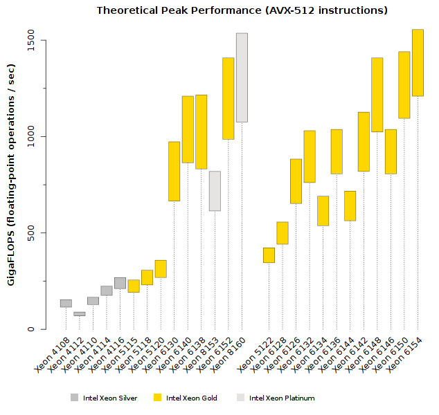
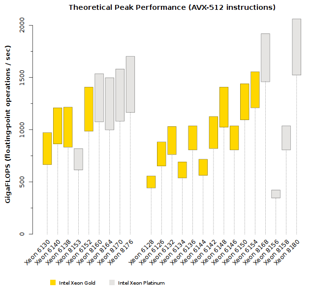
The shaded/colored bars indicate the expected performance ranges for each CPU using the new AVX-512 instructions with FMA. Note that only a small set of codes will be capable of issuing exclusively AVX-512 FMA instructions (e.g., LINPACK). Most applications issue a variety of instructions and will achieve lower than peak FLOPS.
Notice that each plot shows two separate groups of CPUs separated by a gap. The CPU models on the left of each plot offer the highest numbers of CPU cores (with CPU clock frequency being a secondary priority). The CPU models on the right of each plot are optimized for the highest CPU clock speeds (with high CPU core count as the secondary priority). Intel describes these high clock speed models as “optimized for the highest per-core performance”. In previous generations, these “frequency-optimized” CPU models were typically the niche option. However, in this generation the CPU models which offer the highest per-core performance are expected to be the primary choices for HPC users – they provide base clock speeds in the 2GHz~3GHz range. The CPU models which do not prioritize clock speed are in the 1.5GHz~2GHz range, which many HPC users would consider to be too low.
Intel Xeon “Skylake-SP” Price Ranges
Because the pricing of the Xeon Processor Scalable Family spans such a wide range, budgets need to be kept at top of mind when selecting options. It would be frustrating to plan for 28-core processors when the budget cannot support a price of more than $10,000 per CPU.
The tabs below compare the prices of the various CPU tiers. As above, each plot is divided with high-core-count CPUs on the left and highest-per-core performance on the right.
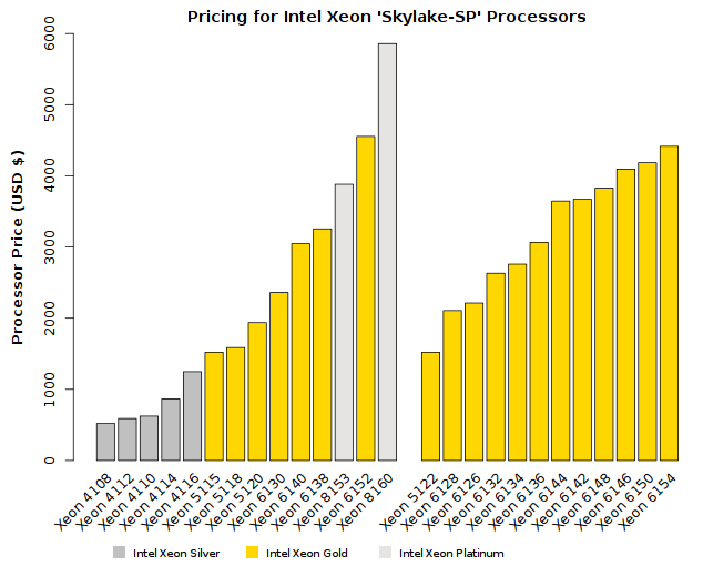
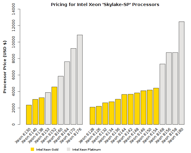
As the above plots show, the CPUs are sorted by price. All of the plots in this article are ordered to match the plots above. Keep the pricing in mind as you review the remainder of the information in this article.
Intel “Skylake-SP” Xeon Processor Scalable Family Specifications
The sets of tabs below compare the features and specifications of this new Xeon processor family. As you will see, the Silver (4100-series) and low-end Gold (5100-series) offer fewer capabilities and lower performance. The high-end Gold (6100-series) and Platinum (8100-series) offer more capabilities and higher performance. Additionally, certain models within the 6100-series and 8100-series have special models integrating additional specializations:
- Enabled for up to 1.5TB of memory per CPU socket (indicated with an M suffix on the part number)
- Including integrated 100Gbps Omni-Path interconnect (indicated with an F suffix on the part number)
In addition to the significant performance increases, there are notable changes to the “Skylake-SP” processor designs. These include a completely new mesh connectivity between the processor cores, redesigned L2/L3 caches, greater connectivity between CPU sockets, and new changes to the processor frequency speeds. These are discussed further in the sections below.
Number of Cores per CPU
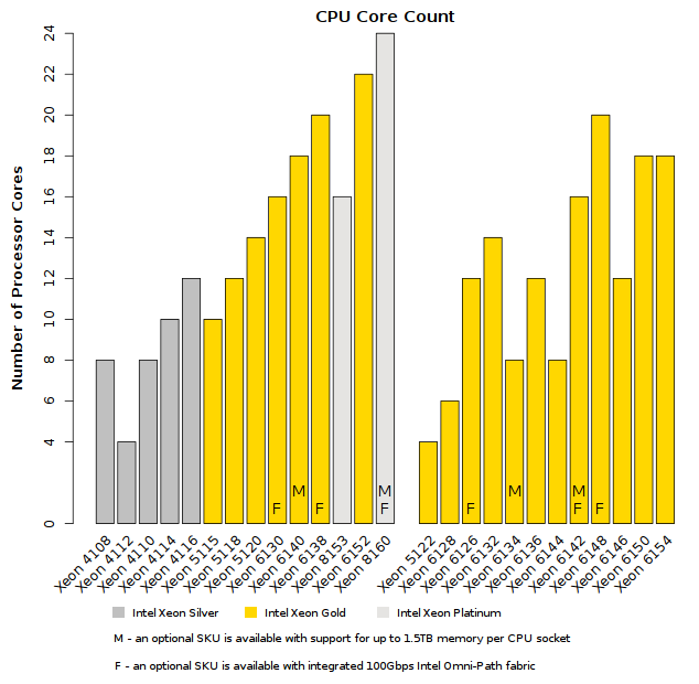
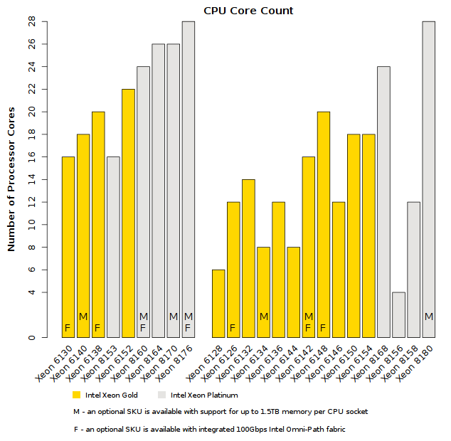
Most HPC groups should find that 12-core, 14-core, and 16-core models fit within their budget. Systems with up to 24-cores per CPU will not be shockingly expensive. However, the 26-core and 28-core models are only available within the Platinum tier and will be at a higher cost than most groups would consider cost-effective.
DDR4 Memory Speed
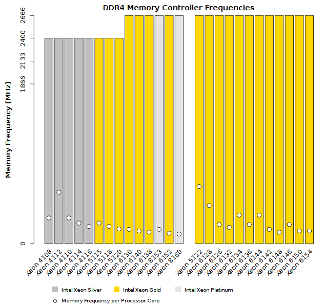
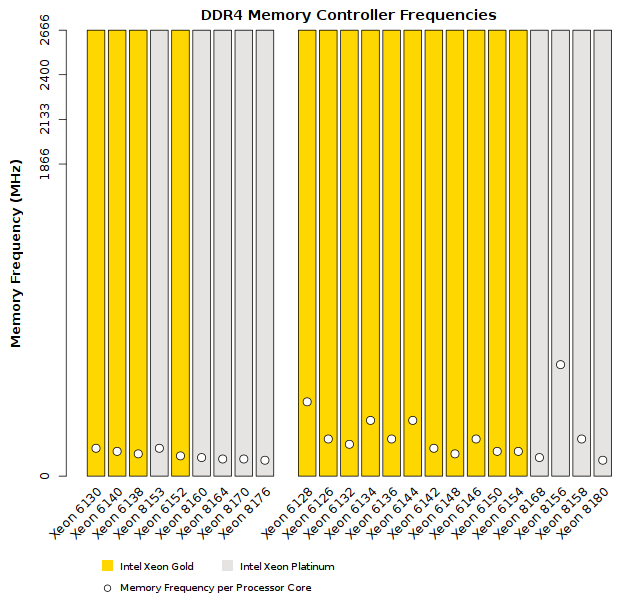
As shown above, memory performance is fairly homogeneous across this CPU family. The amount of memory bandwidth available per CPU core will be an important factor, but is simply a function of the number of cores. Users planning to run on CPUs with higher core counts need to ensure that each core won’t be starved of data.
Intel has also enabled these CPUs to drive fully-populated systems at full memory speed. In previous generations, populating more than half of the memory slots would result in a modest reduction in memory speed.
L3 Cache Size
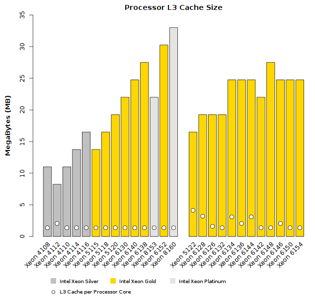
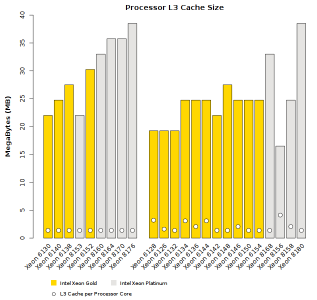
Each CPU has been designed to offer at least 1.375MB of L3 cache per core. As shown above, there are several models which feature a larger quantity of L3 per core. Remember that each core also has 1MB of private L2 cache. In this generation, the L3 cache is largely seen as a fallback if data spills out of L2 (a “victim cache”).
Ultra Path Interconnect (UPI) Performance
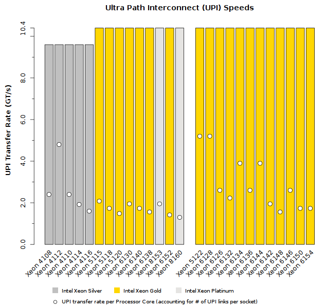
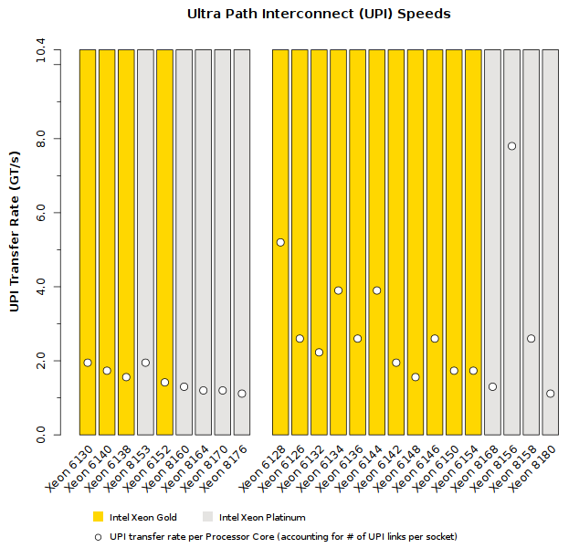
With the “Skylake-SP” architecture, Intel has replaced the older QPI interconnect with UPI. The throughput per link increases from 9.6GT/s to 10.4GT/s. Additionally, many CPU models support up to 3 UPI links per socket (compared to 2 QPI links in most earlier platforms). This allows greater connectivity between sockets, particularly on dual-socket systems which are the most popular configuration for HPC.
Power Consumption (TDP)
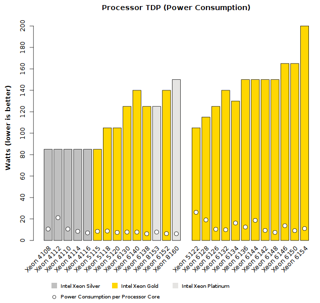
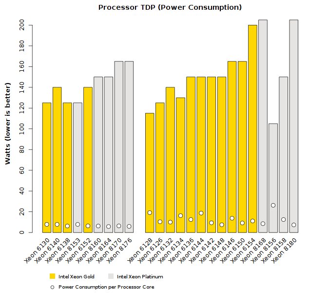
Although there are still many models in the same power range as previous generations, there are an increasing number of models with TDPs above 140 Watts. A couple of models even reach over 200 Watts. For this generation, HPC users must be certain that the systems they use have gone through careful thermal validation. Systems which run warm will suffer lower performance.
Clock Speeds & Turbo Boost in Xeon “Skylake-SP” Scalable Family processors
With each new processor line, Intel introduces new architecture optimizations. The design of the “Skylake-SP” architecture acknowledges that highly-parallel/vectorized applications place the highest load on the processor cores (requiring more power and thus generating more heat). While a CPU core is executing intensive vector tasks (AVX or AVX-512 instructions), the clock speed will be adjusted downwards to keep the processor within its power limits (TDP).
In effect, this will result in the processor running at a lower frequency than the standard clock speed advertised for each model. For that reason, each “Skylake-SP” processor is assigned three “base” frequencies:
- AVX-512 mode: due to the high requirements of AVX-512/FMA instructions, clock speeds will be lowered while executing AVX-512 instructions *
- AVX mode: due to the higher power requirements of AVX2/FMA instructions, clock speeds will be somewhat lower while executing AVX instructions *
- Non-AVX mode: while not executing AVX/AVX-512 instructions, the processor will operate at what would traditionally be considered the “stock” frequency
Each of the “modes” above is actually a range of CPU clock speeds. The CPU will run at the highest speed possible for the particular set of CPU instructions that have been issued. It is worth noting that these modes are isolated to each core. Within a given CPU, some cores may be operating in AVX mode while others are operating in Non-AVX mode.
* Intel has applied a 1-millisecond hysteresis window on each CPU core to prevent rapid frequency transitions
AVX-512, AVX, and Non-AVX Turbo Boost
Just as in previous generations, “Skylake-SP” CPUs include the Turbo Boost feature which allows each processor core to operate well above the “base” clock speed during most operations. The precise clock speed increase depends upon the number & intensity of tasks running on each CPU. However, Turbo Boost speed increases also depend upon the types of instructions (AVX-512, AVX, Non-AVX).
The plots below demonstrate processor clock speeds under the following conditions:
- All cores on the CPU actively running Non-AVX, AVX, or AVX-512 instructions
- A single active core running Non-AVX, AVX, or AVX-512 instructions (all other cores on the CPU must be idle)
The dotted lines represent the range of clock speeds for Non-AVX instructions. The thin cyan bars represent the range of clock speeds for AVX2/FMA instructions. The thicker shaded/colored bars represent the range of clock speeds for AVX-512/FMA instructions.
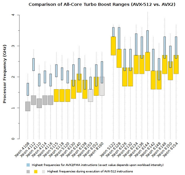
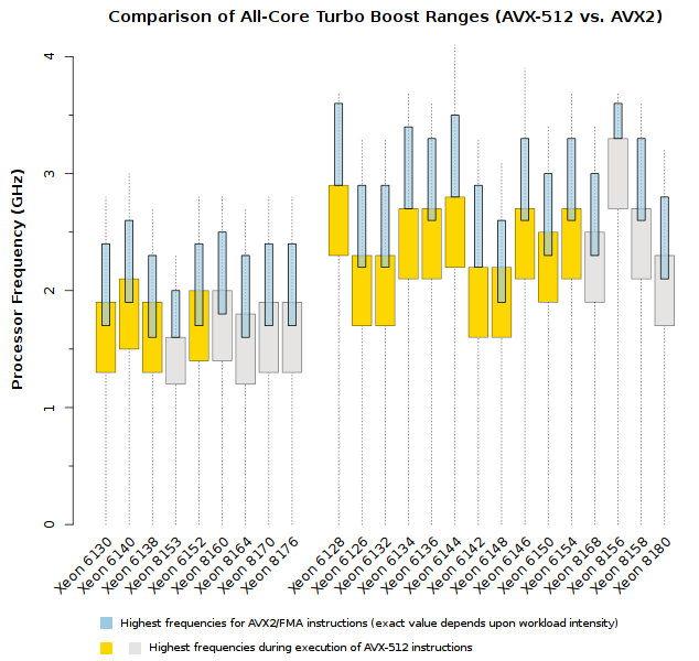
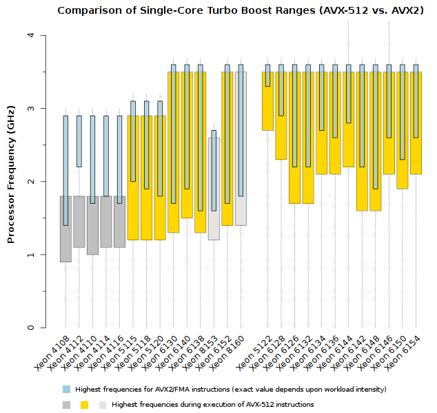
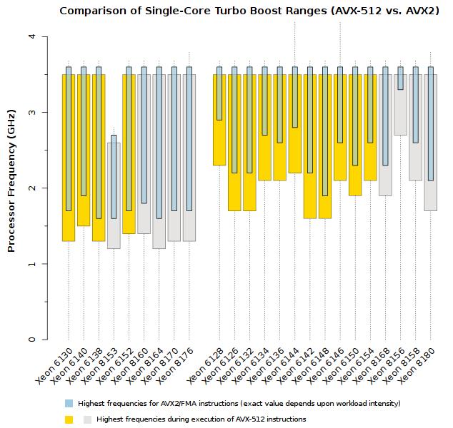
Note that despite the clear rules stated above, each value is still a range of clock speeds. Because workloads are so diverse, Intel is unable to guarantee one specific clock speed for AVX-512, AVX, or Non-AVX instructions. Users are guaranteed that cores will run within a specific range, but each application will have to be benchmarked to determine which frequencies a CPU will operate at.
Despite the perceived reduction in performance when running these vector instructions, keep in mind that AVX-512 roughly doubles the number of operations which can be completed per cycle. Although the clock speeds are reduced, the overall throughput is increased. HPC users should expect their processors to be running in AVX or AVX-512 mode most of the time.
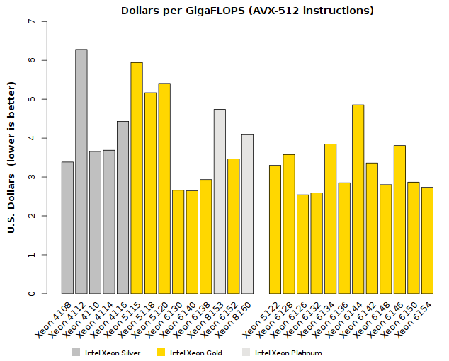
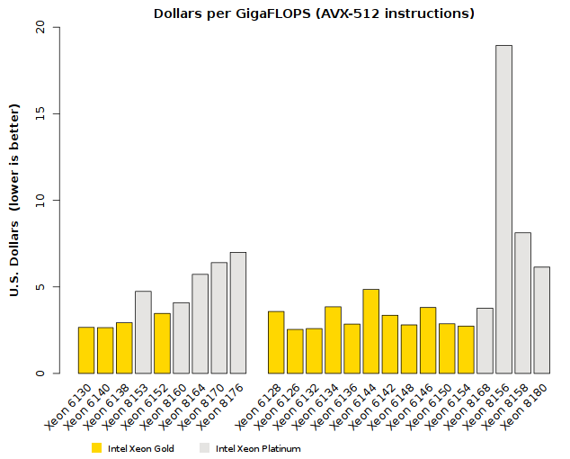
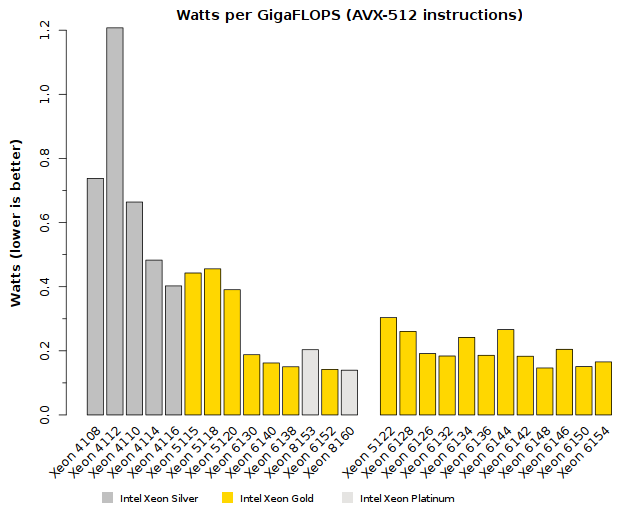
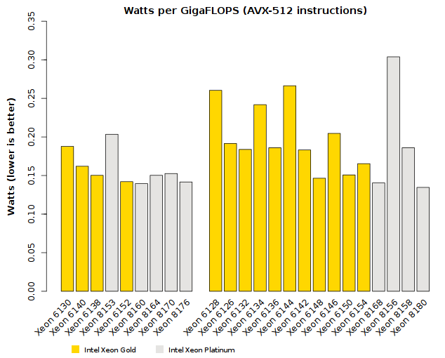
Cost-Effectiveness and Power Efficiency of Xeon “Skylake-SP” CPUs
As mentioned earlier, many of the new processors have the same price structure as earlier Xeon E5 and E7 server CPU families. However, the prices and power requirements for some of the premium models are higher than in previous generations. Savvy readers may find the following facts useful:
- HPC applications run best on the higher-end Gold and Platinum CPU models (6100- and 8100-series), as all of the lower-end CPUs provide only half the number of math units.
- The Platinum models (8100-series) are generally targeted towards Enterprise and Finance – these carry higher prices than other models.
The plots below compare the price versus performance of these CPUs. In general, the Xeon 6100-series provide the most cost-effective performance. The Xeon 4100-series and Xeon 5100-series CPUs are available for a lower price, but they include only a single AVX-512 math unit and do not offer cost-effective performance.
Performance versus Price
The plots below compare the power requirements (TDP) versus performance of each CPU. Although this generation includes some of the highest-wattage CPUs to date, each is actually quite power efficient. In fact, both of the 205 Watt CPU models are among the top three most efficient models in this product line.
Performance versus Power
Summary of features in Xeon Scalable Family “Skylake-SP” processors
In addition to the capabilities mentioned at the top of this article, these processors include many of the successful features from earlier Xeon designs. They also include lower-level changes that may of interest to expert users. The list below provides a more detailed summary of relevant technology features in Skylake-SP:
- Up to 28 processor cores per socket (with options for 4-, 6-, 8-, 10-, 12-, 14-, 16-, 18-, 20-, 24-, and 26-cores)
- Floating Point and Integer Instruction performance improvements:
- New AVX-512 instructions double performance
(up to 16 double-precision FLOPS per cycle per AVX-512 FMA unit) - Up to two AVX-512 FMA units per CPU core (depends upon CPU SKU)
- As introduced with “Haswell” and “Broadwell”, these CPUs continue to support 128-bit AVX and 256-bit AVX2 Advanced Vector Extensions with FMA3
- New AVX-512 instructions double performance
- Memory capacity & performance improvements:
- Six-channel memory controller on each CPU (up from four-channel on previous platforms)
- Support for DDR4 memory speeds up to 2666MHz
- Support for operating DDR4 memory at full speed, even with two memory DIMMs installed per channel
- Optional 1.5TB-per-socket system memory support (only available on certain SKUs)
- Faster links between CPU sockets with up to three 10.4GT/s UPI links (replacing the older QPI interconnect)
- More I/O connectivity with 48 lanes of generation 3.0 PCI-Express per CPU (up from 40 lanes)
- Optional 100Gbps Omni-Path fabric integrated into the processor (only available on certain SKUs)
- CPU cores are arranged in an “Uncore” mesh interconnect (replacing the older dual-ring mesh interconnect)
- Optimized Turbo Boost profiles allow higher frequencies even when many CPU cores are in use
- Direct PCI-Express (generation 3.0) connections between each CPU and peripheral devices such as network adapters, GPUs and coprocessors (48 PCI-E lanes per socket)
- Turbo Boost technology improves performance under peak loads by increasing processor clock speeds. With “Skylake-SP”, clock speeds are boosted higher even when many cores are in use. There are three tiers of Turbo Boost clock speeds depending upon the type of instructions being executed:
- Non-AVX: Operations that are not math intensive, or that use AVX/AVX2 instructions which don’t involve multiply/FMA
- AVX: Operations that heavily use the AVX/AVX2 units, or that use the AVX-512 unit (but not the multiply/FMA instructions)
- AVX-512: Operations that heavily use the AVX-512 units, including multiply/FMA instructions
- Intel QuickData Technology (CBDMA) doubles memory-to-memory copy performance and supports MMIO memory copy
- Intel Volume Management Device (VMD) provides CPU-level device aggregation for NVMe SSD storage devices
- Intel Virtual RAID on CPU (VROC) provides RAID support for NVMe SSD storage devices
- A new Intel C620-series PCH chipset (formerly codenamed “Lewisburg”) with improved connectivity:
- Up to four Intel X722 10GbE/1GbE Ethernet ports with iWARP RDMA support
- PCI-Express generation 3.0 x4 connection from the PCH to the CPUs (previous generations used PCI-E gen 2.0)
- Support for more integrated SATA3 6Gbps ports (up to 14)
- Support for more integrated USB 3.0 ports (up to 10)
- Integrated Intel QuickAssist Technology, which accelerates many cryptographic and compression/decompression workloads
- Enhancements to the CPU Core Microarchitecture:
- Larger and improved branch predictor, higher throughput decoder, larger out-of-order window
- Improved scheduler and execution engine; improved throughput and latency of divide/sqrt
- More load/store bandwidth, deeper load/store buffers, improved prefetcher
- One or Two AVX-512 512-bit FMA units per core (compared to only one on desktop “Skylake” models)
- Support for the following AVX-512 instruction types:
AVX512-F, AVX512-VL, AVX512-BW, AVX512-DQ, AVX512-CD - 1MB L2 cache per core (compared to only 256KB L2 on desktop “Skylake” models)
- A 10% (geomean) improvement in instructions per cycle (IPC) versus the previous-generation Broadwell CPUs
- Re-architected L2/L3 cache hierarchy:
- Each CPU core contains 1MB L2 private cache (up from 256KB)
- Each core’s private L2 acts as primary cache
- Each CPU contains >1.3MB/core of shared L3 cache (for when the private L2 caches overflow)
- The shared L3 cache is now non-inclusive (does not keep copies of the L2 caches)
- Larger 64-entry L2 TLB for 1GB pages (up from 16 entries)
- Dual or Triple Ultra Path Interconnect (UPI) links between processor sockets improve communication speeds for data-intensive applications
- Introduction of the RDSEED instruction for high-quality, non-deterministic, random seed values
- Hyper-Threading technology allows two threads to “share” a processor core for improved resource usage. Although useful for some workloads, it is frequently disabled for HPC applications.
- Hardware Controlled Power Management for more rapid and efficient decisions on optimal P- and C-State operating point