This article provides in-depth discussion and analysis of the 14nm Intel Xeon Processor Scalable Family (formerly codenamed “Cascade Lake-SP” or “Cascade Lake Scalable Processor”). “Cascade Lake-SP” processors replace the previous 14nm “Skylake-SP” microarchitecture and are available for sale as of April 2, 2019. On February 24, 2020, a set of “Cascade Lake Refresh” Xeon models were released with increased clock speeds and improved cost/performance. These Xeon CPUs have been superseded by the 3rd-generation Intel Xeon ‘Ice Lake SP’ scalable processors.
These new CPUs are the second iteration of Intel’s Xeon Processor Scalable Family. They remain compatible with the existing workstation and server platforms, but bring incremental performance along with additional capabilities and options.
Important features/changes in Xeon Scalable Processor Family “Cascade Lake SP” CPUs include:
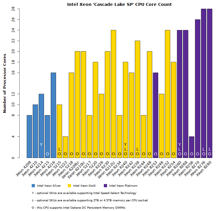
- Up to 28 processor cores per socket (with options for 4-, 6-, 8-, 10-, 12-, 16-, 18-, 20-, 24-, and 26-cores)
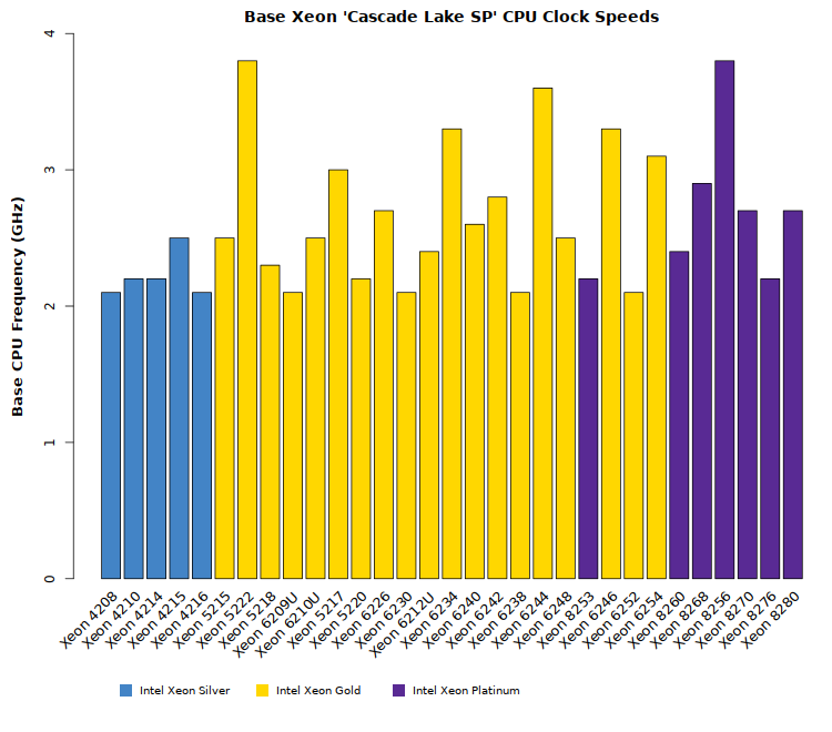
- Improved CPU clock speeds (with Turbo Boost up to 4.4GHz)
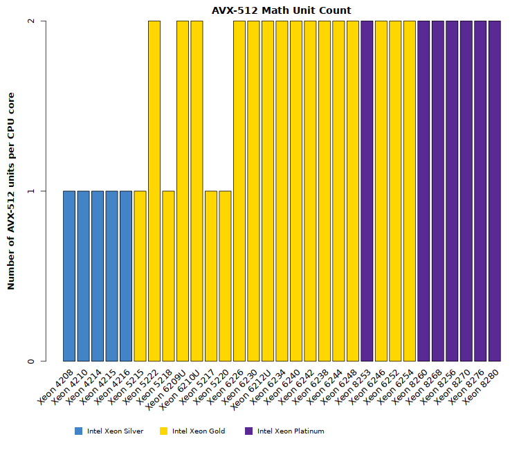
- Continued high performance with the AVX-512 instruction capabilities of the previous generation:
- AVX-512 instructions (up to 16 double-precision FLOPS per cycle per AVX-512 FMA unit)
- Up to two AVX-512 FMA units per CPU core (depends upon CPU SKU)
- Introduction of new AVX-512 VNNI instruction:
- Intel Deep Learning Boost (VNNI) provides significant, more efficient deep learning inference acceleration
- Combines three AVX-512 instructions (VPMADDUBSW, VPMADDWD, VPADDD) into a single VPDPBUSD operation
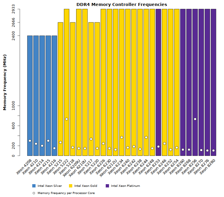
- Memory capacity & performance features:
- Six-channel memory controller on each CPU
- Support for DDR4 memory speeds up to 2933MHz (up from 2666MHz)
- Large-memory capabilities with Intel Optane DC Persistent Memory
- All CPU models support up to 1TB-per-socket system memory
- Optional CPUs support up to 4.5TB-per-socket system memory (only available on certain SKUs)
- Introduction of Intel Speed Select processor models:
- Certain processors support three distinct operating points
- Each operating point provides a different number of CPU cores
- CPU clock and Turbo Boost speeds optimized for each core count
- Integrated hardware-based security mitigations against side-channel attacks
With a product this complex, it’s very difficult to cover every aspect of the design. Here, we concentrate primarily on the performance of the processors for HPC & AI applications.
Specialization of Intel Xeon CPUs
The new “Cascade Lake-SP” processors will be be familiar to existing users. Just as in the previous generation, the processor family is divided into four tiers: Bronze, Silver, Gold, and Platinum. Bronze provides modest performance for a low price. The Silver and Gold models are in the price/performance range familiar to HPC users/architects. Platinum models are in a higher price range than HPC groups are typically accustomed to (Platinum tier targets Enterprise workloads, and is priced accordingly).
However, this new generation is not simply a revision of the previous models. Increasingly, we are seeing processors that have been designed with a particular workload in mind. The “Cascade Lake SP” Xeons introduce several new specialized CPU models:
- S: search optimized
- N: network function virtualization (NFV) optimized
- V: virtualization density optimized
- Y: Intel speed select
- U: single-socket optimized
In the case of the first two specializations (search and NFV), specific CPU clock frequencies and Turbo Boost speeds are guaranteed only for those specific workloads. Running other workloads on these optimized CPUs will likely lead to CPU throttling, which would be undesirable. The virtualization density optimized models provide high CPU core counts within relatively modest power envelopes. However, the processor clock and memory clock frequencies are reduced to accomplish this. Considering these limitations, the search-, NFV-, and virtualization-optimized models will not be included in our review
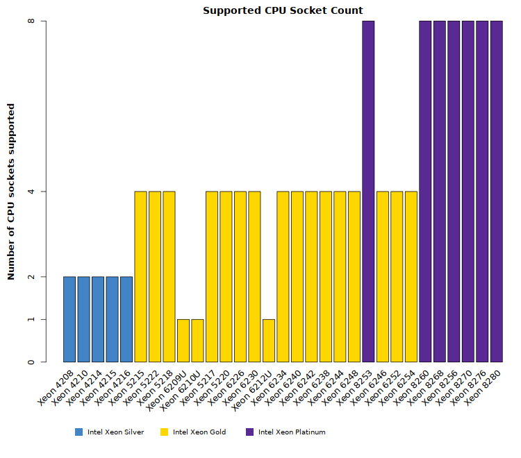
The single-socket optimized CPUs are indicated with a U suffix in the model name (e.g., Xeon 6210U). These CPUs are quite cost-effective for what they offer (a 6200-series CPU for a 5200-series price). However, they do not include UPI links and thus can only be installed in systems with a single processor.
Intel Speed Select CPUs are indicated with a Y suffix in the model name (e.g., Xeon 6240Y). Each of these three CPUs offers the same core count and clock speed as their non-Y counterpart. However, the system can be rebooted into a lower core-count mode which boosts the CPU clock and Turbo Boost speeds. The Speed Select models available in this generation are: 8260Y, 6240Y, and 4214Y. Although these models are not called out by name below, understand that alternate versions of Xeon 8260, 6240, and 4214 are available if you need core count & clock speed flexibility.
Before diving into the details, it helps to keep in mind the following recommendations. Based on our experience with HPC and Deep Learning deployments, our guidance for selecting Xeon tiers is as follows:
- Intel Xeon Bronze – not recommended for HPC
Base-level model with low performance. - Intel Xeon Silver – suitable for entry-level HPC
4200-series models offer slightly improved performance over previous generations. - Intel Xeon Gold – recommended for most HPC workloads
The best balance of performance and price. In particular, the 6200-series models should be preferred over the 5200-series models, because they have twice the number of AVX-512 units - Intel Xeon Platinum – recommended only for specific HPC workloads
Although these 8200-series models provide the highest performance, their higher price makes them suitable only for particular workloads which require their specific capabilities (e.g., high core count, large SMP, and large-memory Compute Nodes).
* Given their positioning, the Intel Xeon Bronze products will not be included in our review
Exceptional Computational Performance
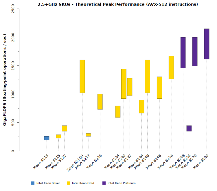
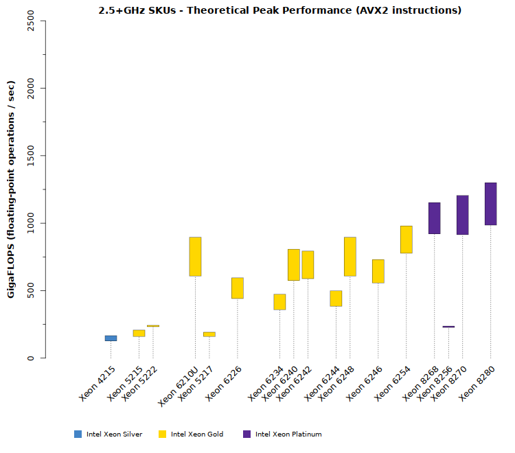
The Xeon “Cascade Lake SP” processors deliver new capabilities and unprecedented performance. Most models provide over 1 TFLOPS (one teraflop of double-precision 64-bit performance per second) and a couple models provide 2 TFLOPS. This performance is achieved with high core counts and AVX-512 instructions with FMA (just as in the previous generation). The plots in the tabs below compare the performance ranges for these new CPUs:
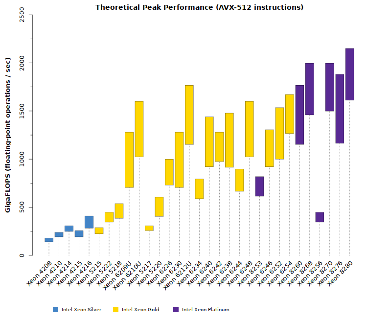
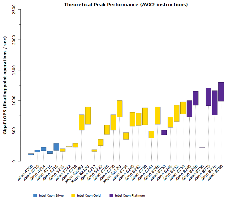
As shown above, the shaded/colored bars indicate the expected performance ranges for each CPU model. The first plot shows performance when using Intel’s AVX-512 instructions with FMA. Note that only a small set of codes will be capable of issuing exclusively AVX-512 FMA instructions (e.g., LINPACK). Most applications issue a variety of instructions and will achieve lower than peak FLOPS. Applications which have not been re-compiled with an appropriate compiler will not include AVX-512 instructions and thus achieve lower performance. Those expected performance ranges are shown in the plot of AVX2 Instruction performance.
Although the ordering of the above plots may seem arbitrary, they are sorted by price (as discussed in the next section). The lowest-performance models provide fewer numbers of CPU cores and fewer AVX math units. Higher-end models provide a mix of higher core counts and higher clock speeds. A few CPU models, such as Xeon 6244 and Xeon 8256, strongly favor high clock speeds over CPU core count (which results in lower overall FLOPS throughput). HPC and AI groups are expected to favor the Intel Xeon Gold processor models.
Intel Xeon “Cascade Lake SP” Price Ranges
The pricing of the Xeon Processor Scalable Family spans a wide range, so budget must be kept at top of mind when selecting options. It would be frustrating to plan for 28-core processors when the budget cannot support a price of more than $10,000 per CPU. The plot below compares the prices of the Xeon “Cascade Lake SP” processors:
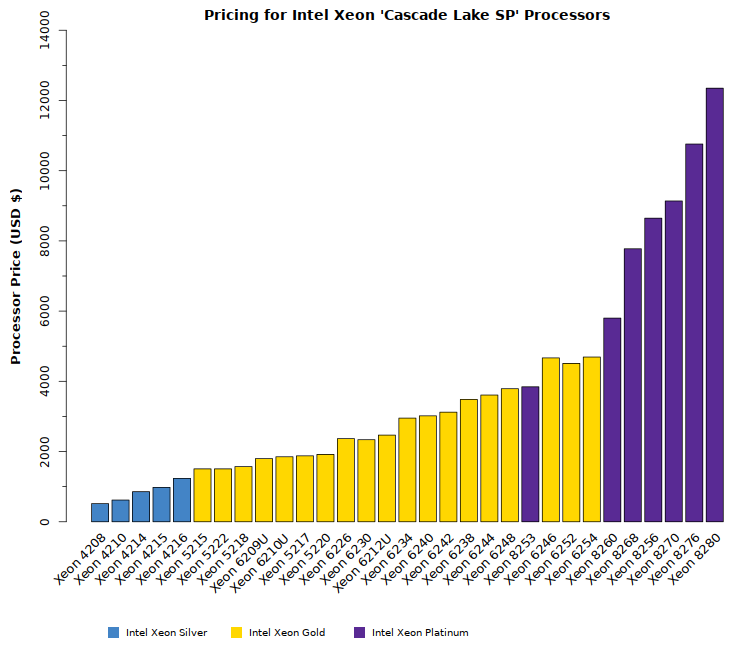
As in the above plot, all the CPUs in this article are sorted by price. Most HPC users are expected to select CPU models from the Gold Xeon 6200-series. These models provide close to peak performance for a price under $4,000 per processor. Certain specialized applications will leverage the Platinum Xeon 8200-series, such as very large memory nodes (>3TB system memory).
To ease comparisons, all of the plots in this article are ordered to match the above plot. Keep this pricing in mind as you review this article and plan your system architecture.
Intel “Cascade Lake SP” Xeon Processor Scalable Family Specifications
The sets of tabs below compare the features and specifications of this new Xeon processor family. As you will see, the Silver (4200-series) and lower-end Gold (5200-series) CPU models offer fewer capabilities and lower performance. The higher-end Gold (6200-series) and Platinum (8200-series) offer more capabilities and higher performance. Additionally, certain CPU SKUs have special models integrating additional specializations:
- Enabled for Intel Speed Select (indicated with a Y suffix on the part number)
- Support for up to 4.5TB of memory per CPU socket (indicated with an L suffix on the part number)
(these same CPUs have a lower-cost alternate SKU supporting 2TB memory per socket (indicated with an M suffix on the part number) - Designed for single CPU socket systems (indicated with a U suffix on the part number)
- All Gold- and Platinum-series CPUs support Intel’s new Optane DC Persistent Memory
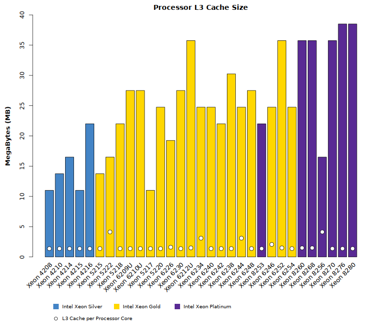
In addition to the specifications called out above, technical readers should note that the “Cascade Lake SP” CPU architecture inherits most of the architectural design of the previous “Skylake-SP” architecture, including the mesh processor layout, redesigned L2/L3 caches, greater UPI connectivity between CPU sockets, and improvements to the processor frequency speeds/turbo. A more comprehensive list of features is shown at the end of the article.
Clock Speeds & Turbo Boost
Just as in the previous generation, the “Cascade Lake-SP” architecture acknowledges that highly-parallel/vectorized applications place the highest load on the processor cores (requiring more power and generating more heat). While a CPU core is executing intensive vector tasks (AVX2 or AVX-512 instructions), the clock speed will be adjusted downwards to keep the processor within its power limits (TDP).
In effect, this will result in the processor running at a lower frequency than the standard clock speed advertised for each model. For that reason, each processor is assigned three frequency ranges:
- AVX-512 mode: due to the high requirements of AVX-512/FMA instructions, clock speeds will be lowered while executing AVX-512 instructions *
- AVX2 mode: due to the higher requirements of AVX2/FMA instructions, clock speeds will be somewhat lower while executing AVX instructions *
- Non-AVX mode: while not executing “heavy” AVX instructions, the processor will operate at the “stock” frequency
Each of the “modes” above is actually a range of CPU clock speeds. The CPU will run at the highest speed possible for the particular set of CPU instructions that have been issued. It is worth noting that these modes are isolated to each core. Within a given CPU, some cores may be operating in AVX mode while others are operating in Non-AVX mode.
* Intel has applied a 1-millisecond hysteresis window on each CPU core to prevent rapid frequency transitions
AVX-512, AVX, and Non-AVX Turbo Boost in Xeon “Cascade Lake-SP” Scalable Family processors
Each CPU also includes the Turbo Boost feature which allows each processor core to operate well above the “base” clock speed during most operations. The precise clock speed increase depends upon the number & intensity of tasks running on each CPU. However, Turbo Boost speed increases also depend upon the types of instructions (AVX-512, AVX, Non-AVX).
The plots below demonstrate processor clock speeds under the following conditions:
- All cores on the CPU actively running Non-AVX, AVX, or AVX-512 instructions
- A single active core running Non-AVX, AVX, or AVX-512 instructions (all other cores on the CPU must be idle)
The dotted lines represent the range of clock speeds for Non-AVX instructions. The thin grey bars represent the range of clock speeds for AVX2/FMA instructions. The thicker shaded/colored bars represent the range of clock speeds for AVX-512/FMA instructions.
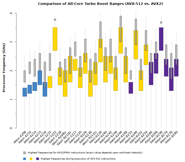
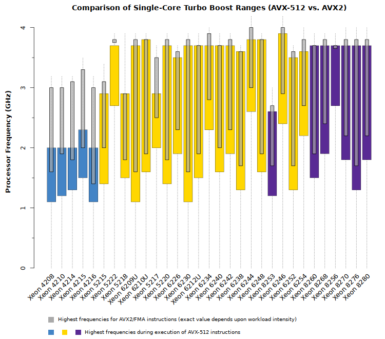
Note that despite the clear rules stated above, each Turbo Boost value is still a range of clock speeds. Because workloads are so diverse, Intel is unable to guarantee one specific clock speed for AVX-512, AVX, or Non-AVX instructions. Users are guaranteed that cores will run within a specific range, but each application will have to be benchmarked to determine which frequencies a CPU will operate at.
Despite the perceived reduction in performance when running these vector instructions, keep in mind that AVX-512 roughly doubles the number of operations which can be completed per cycle. Although the clock speeds might be reduced by nearly 1GHz, the overall throughput is increased. HPC users should expect their processors to be running in AVX or AVX-512 mode most of the time.
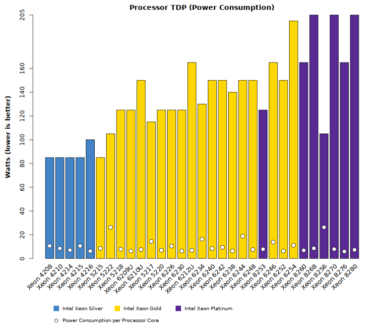
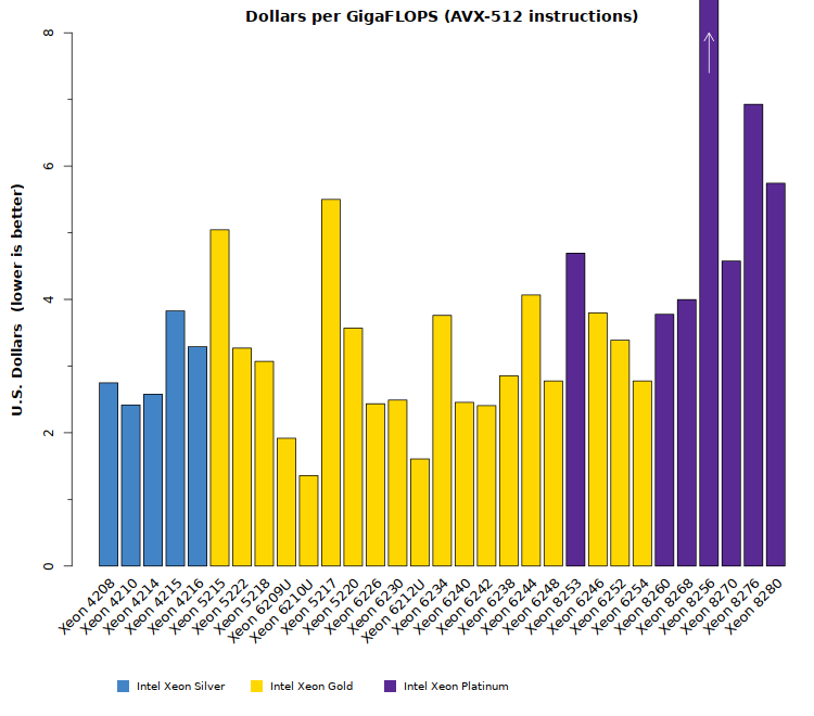
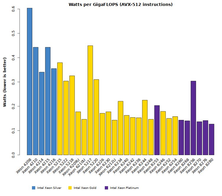
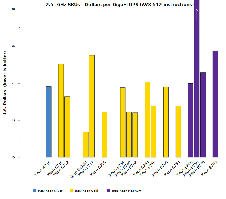
Cost-Effectiveness and Power Efficiency of Xeon “Cascade Lake SP” CPUs
Many of these new processors have the same price structure as earlier Xeon server CPU families. However, the prices and power requirements for some of the premium models are fairly high. Savvy readers may find the following facts useful:
- HPC applications run best on the higher-end Gold and Platinum CPU models (6200- and 8200-series), as all of the lower-end CPUs provide only half the number of math units.
- Applications which can be satisfied by a single CPU will benefit greatly from the single-socket Xeon 62xxU models
- The Platinum models (8200-series) are generally targeted towards Enterprise and Finance – these carry higher prices than other models.
The plots below compare the cost-effectiveness and power efficiency of these CPU models. The intent is to go beyond the raw “speeds and feeds” of the processors to determine which models will be most attractive for HPC and Deep Learning/AI deployments.
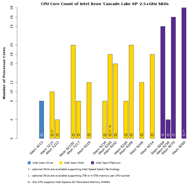
Recommended CPU Models for HPC & AI/Deep Learning
Although many of these CPU models will offer excellent performance, it is common for HPC sites to set a floor on CPU clock speeds (usually around 2.5GHz). The intent is to ensure that no workload suffers too low of a performance. While there are users who would prefer higher clock speeds, experience shows that most groups settle on a value of 2.5GHz to 2.6GHz. With that in mind, the comparisons below highlight only those CPU models which offer 2.5+GHz performance.
Summary of features in Xeon Scalable Family “Cascade Lake-SP” processors
In addition to the capabilities mentioned at the top of this article, these processors include many of the successful features from earlier Xeon designs. They also include lower-level changes that may of interest to expert users. The list below provides a more detailed summary of relevant technology features in Cascade Lake-SP:
- Up to 28 processor cores per socket (with options for 4-, 6-, 8-, 10-, 12-, 16-, 18-, 20-, 24-, and 26-cores)
- Improved CPU clock speeds (with Turbo Boost up to 4.4GHz)
- Continued high performance with the AVX-512 instruction capabilities of the previous generation:
- AVX-512 instructions (up to 16 double-precision FLOPS per cycle per AVX-512 FMA unit)
- Up to two AVX-512 FMA units per CPU core (depends upon CPU SKU)
- Introduction of new AVX-512 VNNI instruction:
- Intel Deep Learning Boost – the new 8-bit Vector Neural Network Instruction (VNNI) provides significant, more efficient deep learning inference acceleration
- Combines three AVX-512 instructions (VPMADDUBSW, VPMADDWD, VPADDD) into a single VPDPBUSD operation
- As introduced with “Haswell” and “Broadwell”, these CPUs continue to support 128-bit AVX and 256-bit AVX2 Advanced Vector Extensions with FMA3
Memory capacity & performance features:
- Six-channel memory controller on each CPU
- Support for DDR4 memory speeds up to 2933MHz (up from 2666MHz)
- Single DIMM per channel operates at up to 2933MHz; two DIMMs per channel operate at up to 2666MHz
- Large-memory capabilities with Intel Optane DC Persistent Memory
- All CPU models support up to 1TB-per-socket system memory
- Optional CPU support for 2TB- or 4.5TB-per-socket system memory (only available on certain SKUs)
Introduction of Intel Speed Select processor models:
- Certain processors support three distinct operating points
- Each operating point provides a different number of CPU cores
- CPU clock and Turbo Boost speeds optimized for each core count
- Integrated hardware-based security mitigations against side-channel attacks
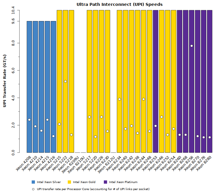
- Fast links between CPU sockets with up to three 10.4GT/s UPI links
- I/O connectivity of 48 lanes of generation 3.0 PCI-Express per CPU
- CPU cores are arranged in an “Uncore” mesh interconnect
- Optimized Turbo Boost profiles allow higher frequencies even when many CPU cores are in use
- Direct PCI-Express (generation 3.0) connections between each CPU and peripheral devices such as network adapters, GPUs and coprocessors (48 PCI-E lanes per socket)
- Turbo Boost technology improves performance under peak loads by increasing processor clock speeds. Clock speeds are boosted higher even when many cores are in use. There are three tiers of Turbo Boost clock speeds depending upon the type of instructions being executed:
- Non-AVX: Operations that are not math intensive, or “light” AVX/AVX2 instructions which don’t involve multiply/FMA
- AVX: Operations that heavily use the AVX/AVX2 units, or that use the AVX-512 unit (but not the multiply/FMA instructions)
- AVX-512: Operations that heavily use the AVX-512 units, including multiply/FMA instructions
- Intel QuickData Technology (CBDMA) doubles memory-to-memory copy performance and supports MMIO memory copy
- Intel Volume Management Device (VMD) provides CPU-level device aggregation for NVMe SSD storage devices
- Intel Virtual RAID on CPU (VROC) provides RAID support for NVMe SSD storage devices
- Intel C620-series PCH chipset (formerly codenamed “Lewisburg”) with improved connectivity:
- Up to four Intel X722 10GbE/1GbE Ethernet ports with iWARP RDMA support
- PCI-Express generation 3.0 x4 connection from the PCH to the CPUs
- Support for more integrated SATA3 6Gbps ports (up to 14)
- Support for more integrated USB 3.0 ports (up to 10)
- Integrated Intel QuickAssist Technology, which accelerates many cryptographic and compression/decompression workloads
- Enhanced CPU Core Microarchitecture:
- Larger and improved branch predictor, higher throughput decoder, larger out-of-order window
- Improved scheduler and execution engine; improved throughput and latency of divide/sqrt
- More load/store bandwidth, deeper load/store buffers, improved prefetcher
- One or Two AVX-512 512-bit FMA units per core
- Support for the following AVX-512 instruction types:
AVX512-F, AVX512-VL, AVX512-BW, AVX512-DQ, AVX512-CD - 1MB dedicated L2 cache per core
- A 10% (geomean) improvement in instructions per cycle (IPC) versus the “Broadwell” generation CPUs
- Re-architected L2/L3 cache hierarchy:
- Each CPU core contains 1MB L2 private cache (up from 256KB)
- Each core’s private L2 acts as primary cache
- Each CPU contains >1.3MB/core of shared L3 cache (for when the private L2 cache is exhausted)
- The shared L3 cache is non-inclusive (does not keep copies of the L2 caches)
- Larger 64-entry L2 TLB for 1GB pages (up from 16 entries)
- Dual or Triple Ultra Path Interconnect (UPI) links between processor sockets improve communication speeds for data-intensive applications
- RDSEED instruction for high-quality, non-deterministic, random seed values
- Hyper-Threading technology allows two threads to “share” a processor core for improved resource usage. Although useful for some workloads, it is frequently disabled for HPC applications.
- Hardware Controlled Power Management for more rapid and efficient decisions on optimal P- and C-State operating point