This article provides in-depth discussion and analysis of the 10nm Intel Xeon Processor Scalable Family (formerly codenamed “Ice Lake-SP” or “Ice Lake Scalable Processor”). These processors replace the previous 14nm “Cascade Lake-SP” microarchitecture and are available for sale as of April 6, 2021.
The “Ice Lake SP” CPUs are the 3rd generation of Intel’s Xeon Scalable Processor family. This generation brings new features, increased performance, and new server/workstation platforms. The Xeon ‘Ice Lake SP’ CPUs cannot be installed into previous-generation systems. Those considering a new deployment are encouraged to review with one of our experts.
Highlights of the features in Xeon Scalable Processor Family “Ice Lake SP” CPUs include:
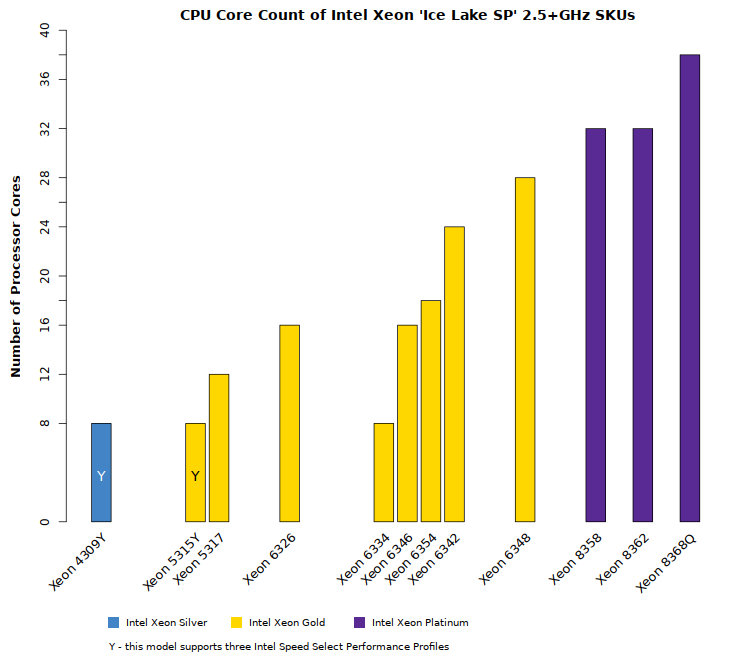
- Up to 40 processor cores per socket (with options for 8-, 12-, 16-, 18-, 20-, 24-, 26-, 28-, 32-, 36-, and 38-cores)
- Up to 38% higher per-core performance through micro-architecture improvements (at same clock speed vs “Cascade Lake SP”)
- Significant memory performance & capacity increases:
- Eight-channel memory controller on each CPU (up from six)
- Support for DDR4 memory speeds up to 3200MHz (up from 2933MHz)
- Large-memory capacity with Intel Optane Persistent Memory
- All CPU models support up to 6TB per socket (combined system memory and Optane persistent memory)
- Increased link speed between CPU sockets: 11.2GT/s UPI links (up from 10.4GT/s)
- I/O Performance Improvements – more than twice the throughput of “Cascade Lake SP”:
- PCI-Express generation 4.0 doubles the throughput of each PCI-E lane (compared to gen 3.0)
- Support for 64 PCI-E lanes per CPU socket (up from 48 lanes)
- Continued high performance with the AVX-512 instruction capabilities of the previous generation:
- AVX-512 instructions (up to 16 double-precision FLOPS per cycle per AVX-512 FMA unit)
- Two AVX-512 FMA units per CPU core (available in all Ice Lake-SP CPU SKUs)
- Continued support for deep learning inference with AVX-512 VNNI instruction:
- Intel Deep Learning Boost (VNNI) provides significant, more efficient deep learning inference acceleration
- Combines three AVX-512 instructions (VPMADDUBSW, VPMADDWD, VPADDD) into a single VPDPBUSD operation
- Improvements to Intel Speed Select processor configurability:
- Performance Profiles: certain processors support three distinct core count/clock speed operating points
- Base Frequency: specific CPU cores are given higher base clock speeds; the remaining cores run at lower speeds
- Turbo Frequency: specific CPU cores are given higher turbo-boost speeds; the remaining cores run at lower speeds
- Core Power: each CPU core is prioritized; when surplus frequency is available, it is given to high-priority cores
- Integrated hardware-based security improvements and total memory encryption
With a product this complex, it’s very difficult to cover every aspect of the design. Here, we concentrate primarily on the performance of the processors for HPC & AI applications.
Continued Specialization of Xeon CPU SKUs
Those already familiar with Intel Xeon will see this processor family is divided into familiar tiers: Silver, Gold, and Platinum. The Silver and Gold models are in the price/performance range familiar to HPC/AI teams. Platinum models are in a higher price range. The low-end Bronze tier present in previous generations has been dropped.
Further, Intel continues to add new specialized CPU models that are optimized for particular workloads and environments. Many of these specialized SKUs are not relevant to readers here, but we summarize them briefly:
- N: network function virtualization (NFV) optimized
- P: virtualization-optimized (with a focus on clock frequency)
- S: max SGX enclave size
- T: designed for higher-temperature environments (NEBS)
- V: virtualization-optimized (with focus on high-density/low-power)
Targeting specific workloads and environments provides the best performance and efficiency for those use cases. However, using these CPUs for other workloads may reduce performance, as the CPU clock frequencies and Turbo Boost speeds are guaranteed only for those specific workloads. Running other workloads on these optimized CPUs will likely lead to CPU throttling, which would be undesirable. Considering these limitations, the above workload-optimized models will not be included in our review.
Four Xeon CPU specializations relevant to HPC & AI use cases
There are several specialized Xeon CPU options which are relevant to high performance computationally-intensive workloads. Each capability is summarized below and included in our analysis.
- Liquid-cooled – Xeon 8368Q CPU: optimized for liquid-cooled deployment, this CPU SKU offers high core counts along with higher CPU clock frequencies. The high clock frequencies are made possible only through the more effective cooling provided by liquid-cooled datacenters.
- Media, AI, and HPC – Xeon 8352M CPU: optimized for AVX-heavy vector instruction workloads as found in media processing, AI, and HPC; this CPU SKU offers improved performance per watt.
- Performance Profiles – Y: a set of CPU SKUs with support for Intel Speed Select Technology – Performance Profiles. These CPUs are indicated with a Y suffix in the model name (e.g., Xeon 8352Y) and provide flexibility for those with mixed workloads. Each CPU supports three different operating profiles with separate CPU core count, base clock and turbo boost frequencies, as well as operating wattages (TDP). In other words, each CPU could be thought of as three different CPUs. Administrators switch between profiles via system BIOS, or through Operating Systems with support for this capability (Intel SST-PP). Note that several of the other specialized CPU SKUs also support multiple Performance Profiles (e.g., Xeon 8352M).
- Single Socket – U: single-socket optimized. The CPUs designed for a single socket are indicated with a U suffix in the model name (e.g., Xeon 6312U). These CPUs are more cost-effective. However, they do not include UPI links and thus can only be installed in systems with a single processor.
Summary of Xeon “Ice Lake-SP” CPU tiers
With the Bronze CPU tier no longer present, all models in this CPU family are well-suited to HPC and AI (though some will offer more performance than others). Before diving into the details, we provide a high-level summary of this Xeon processor family:
- Intel Xeon Silver – suitable for entry-level HPC
The Xeon Silver 4300-series CPU models provide higher core counts and increased memory throughput compared to previous generations. However, their performance is limited compared to Gold and Platinum (particularly on Core Count, Clock Speed, Memory Performance, and UPI speed). - Intel Xeon Gold – recommended for most HPC workloads
Xeon Gold 5300- and 6300-series CPUs provide the best balance of performance and price. In particular, the 6300-series models should be preferred over the 5300-series models, because the 6300-series CPUs offer improved Clock Speeds and Memory Performance. - Intel Xeon Platinum – only for specific HPC workloads
Although 8300-series models provide the highest performance, their higher price makes them suitable only for particular workloads which require their specific capabilities (e.g., highest core count, large L3 cache).
Xeon “Ice Lake SP” Computational Performance
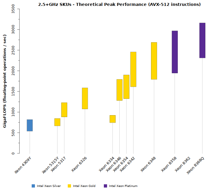
With this new family of Xeon processors, Intel once again delivers unprecedented performance. Nearly every model provides over 1 TFLOPS (one teraflop of double-precision 64-bit performance per second), many models exceed 2 TFLOPS, and a few touch 3 TFLOPS. These performance levels are achieved through high core counts and AVX-512 instructions with FMA (as in the first and second Xeon Scalable generations). The plots in the tabs below compare the performance ranges for these new CPUs:
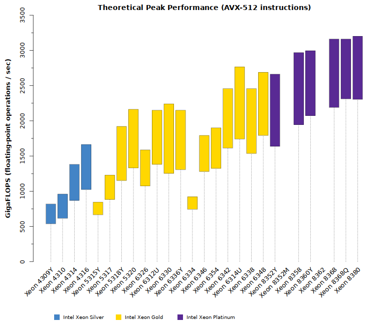
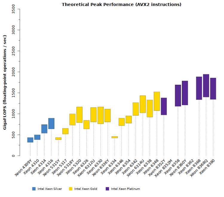
In the charts above, the shaded/colored bars indicate the expected performance range for each CPU model. The performance is a range rather than a specific value, because CPU clock frequencies scale up and down on a second-by-second basis. The precise achieved performance depends upon a variety of factors including temperature, power envelope, type of cooling technology, the load on each CPU core, and the type(s) of CPU instructions being issued to each core.
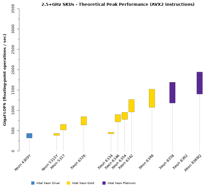
The first tab shows performance when using Intel’s AVX-512 instructions with FMA. Note that only a small set of codes will be capable of issuing exclusively AVX-512 FMA instructions (e.g., HPL LINPACK). Most applications issue a mix of instructions and will achieve lower than peak FLOPS. Further, applications which have not been re-compiled with an appropriate compiler will not include AVX-512 instructions and thus achieve lower performance. Computational applications which do not utilize AVX-512 instructions will most likely utilize AVX2 instructions (as shown in the second tab with AVX2 Instruction performance.
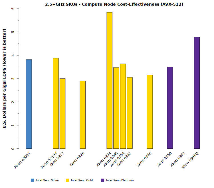
Intel Xeon “Ice Lake SP” Price Ranges
The pricing of the 3rd-generation Xeon Processor Scalable Family spans a wide range, so budget must be kept in mind when selecting options. It would be frustrating to plan on 38-core processors when the budget cannot support a price of more than $10,000 per CPU. The plot below compares the prices of the Xeon “Cascade Lake SP” processors:
As shown in the above plot, the CPUs in this article have been sorted by tier and by price. Most HPC users are expected to select CPU models from the Gold Xeon 6300-series. These models provide close to peak performance for a price around $3,000 per processor. Certain specialized applications will leverage the Platinum Xeon 8300-series
To ease comparisons, all of the plots in this article are ordered to match the above plot. Keep this pricing in mind as you review this article and plan your system architecture.
Recommended Xeon CPU Models for HPC & AI/Deep Learning
As stated at the top, most of this new CPU family offers excellent performance. However, it is common for HPC sites to set a minimum floor on CPU clock speeds (usually around 2.5GHz), with the intent that no workload suffers too low of a performance. While there are users who would demand even higher clock speeds, experience shows that most groups settle on a minimum clock speed in the 2.5GHz to 2.6GHz range. With that in mind, the comparisons below highlight only those CPU models which offer 2.5+GHz performance.